
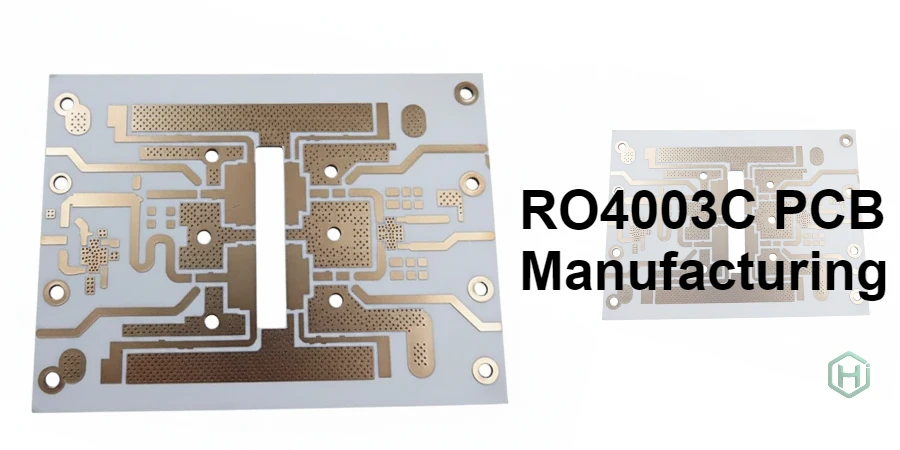
When searching for RO4003C PCB China, professionals are often seeking a reliable and experienced manufacturer capable of delivering high-quality, high-frequency PCBs that meet specific design and performance requirements. At HILPCB, we specialize in advanced PCB manufacturing, including high-frequency and hybrid PCBs that incorporate materials like RO4003C.
As a leading Chinese PCB manufacturer, HILPCB offers a comprehensive range of services, from high-precision PCB fabrication to complete assembly solutions. We are experienced in designing and producing high-frequency PCBs with controlled impedance, optimal stackups, and consistent performance for applications such as RF, microwave, and high-speed digital systems. Whether you need a prototype or large-scale production, HILPCB ensures consistent, export-quality results for your most demanding projects.
1. RO4003C PCB China in the Global RF Supply Chain
RO4003C has become a common choice for RF and microwave designs because it offers a practical balance between performance and manufacturability. In the context of RO4003C PCB China projects, it is often used as part of a broader high-frequency portfolio that also includes PTFE-based laminates and other engineered substrates.
From China, HILPCB ships RO4003C-based PCBs and assemblies to customers in:
- Wireless infrastructure and small cells
- High-frequency radar and sensing
- Satcom, point-to-point microwave links and RF front-ends
- Mixed-signal and high-speed digital systems where RF and digital logic share one platform
Instead of limiting a design to a single laminate, we position RO4003C alongside other high-frequency options within our high-frequency PCB manufacturing service, so each layer and function can be assigned the most suitable material.
2. Stackup Strategies for RO4003C PCB China Projects
A typical RO4003C PCB China order does not consist of a simple two-layer board. Most RF and mixed-signal designs are multilayer, combining RF, high-speed, control and power domains within one structure.
At HILPCB, stackup planning covers:
- Layer allocation for RF traces, shield planes, digital signals and power distribution
- Selection of RO4003C core thicknesses to match characteristic impedance targets
- Integration with FR-4 or other materials when a hybrid structure is required
- Copper weight choices based on current, loss and thermal considerations
In practice, many of these designs end up as multilayer PCBs where RO4003C is used only where its RF properties are needed, while other layers use more cost-effective materials. This allows engineers to keep total board cost under control without compromising RF performance.
3. Transmission Lines, Impedance and Loss Control
For RO4003C PCB China projects, signal integrity is one of the most important concerns. HILPCB supports a range of transmission line structures on RO4003C, including:
- Microstrip lines on outer layers for antennas, matching networks and RF routing
- Stripline structures inside the stackup for protected high-speed channels
- Grounded coplanar waveguide (GCPW) for compact routing and improved isolation
- Differential pairs and coupled lines for filters and high-speed serial interfaces
In order to reach target impedances and predictable loss figures, our engineering team considers:
- Effective dielectric constant for each configuration
- Finished copper thickness (base copper plus plating)
- Solder mask coverage and its impact on impedance
- Dimensional tolerances for line width and spacing in mass production
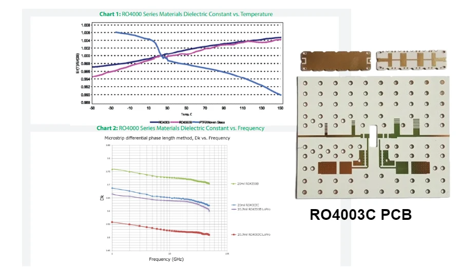
RO4003C’s controlled Dk and low loss tangent provide a solid foundation for this work, while our process control keeps manufacturing variation within a window that high-frequency designs can tolerate.
4. Material Portfolio: Beyond RO4003C
Although this page focuses on RO4003C PCB China, most real products require more than one material family. HILPCB maintains a material portfolio that allows engineers to combine RO4003C with other RF laminates and standard FR-4 depending on the performance and cost targets.
Examples include:
- RO4003C signal layers coupled with PTFE-based or other low-loss dielectrics for ultra-low-loss sections
- Hybrid RF + digital stacks where RF layers use specialized laminates and logic layers use FR-4
- Designs where dielectric properties differ between zones and functions
Engineers working with PTFE-insulated structures can explore our Teflon PCB options, while more general laminate combinations are described in our Rogers PCB manufacturing capability. In all cases, HILPCB works to match material selection with the electrical and mechanical goals of the complete assembly.
5. Manufacturing Flow for RO4003C PCB China Orders
The production flow for RO4003C PCB China projects is designed to support both performance and export logistics.
Key elements include:
- Data intake and engineering review – We review stackup, controlled-impedance nets, critical RF structures and any hybrid material requirements.
- Panelization and tooling – Panels are optimized for yield, RF connector positions and mechanical constraints, while allowing for test coupons where required.
- Lamination and drilling – Parameters are tuned for RO4003C and any companion materials to ensure layer registration, reliable vias and stable dielectric behavior.
- Patterning and surface finish – Etching processes are managed to maintain line geometry, followed by surface finishes chosen for frequency range and assembly profile.
- Inspection and electrical test – Boards are subjected to electrical test, and additional impedance or RF test structures can be implemented if specified.
This flow is applied not only to RO4003C but also to other high-frequency laminates used in the same stack.
6. Assembly Options for RO4003C PCB China Projects
For many customers, a RO4003C PCB China order includes not only bare boards but also full or partial assembly. HILPCB provides flexible assembly options to match the stage of your product lifecycle.
6.1 Prototypes and Engineering Builds
During design validation, the emphasis is on flexibility and rapid feedback:
- Support for component substitutions when specific packages or RF parts are temporarily unavailable
- Close communication on stencil design, reflow profile and handling requirements
- Quick iteration on RF layout and stackup if tuning is needed
For early runs, customers often combine RO4003C boards with our small-batch assembly service to keep development cycles short.
6.2 Ramps and Volume Production
Once the design is stable, attention shifts to repeatability and throughput. HILPCB’s large-volume assembly capability supports RO4003C PCB China projects entering mass production, including:
- High-mix or high-volume SMT lines with inline AOI
- Process windows tuned to protect high-frequency laminates during multiple reflow cycles
- Traceability options for critical assemblies
Depending on the project, we can maintain the same bill-of-materials from prototype to production or support controlled component substitutions where appropriate.
6.3 From PCB to Finished Unit
Some programs require more than a populated circuit board. HILPCB can extend RO4003C PCB China projects into:
- Mechanical integration, cabling and installation of RF shields and connectors
- System-level assembly and packaging
- Final inspection and test according to customer procedures
These services are organized under our box-build assembly and turnkey assembly offerings, allowing hardware teams to work with a single partner from bare boards to finished electronic units.
7. Typical RO4003C PCB China Applications Served by HILPCB
The combination of RO4003C, hybrid stackups and scalable assembly makes HILPCB suitable for a wide range of RO4003C PCB China applications, such as:
- Dual-band WLAN front-end modules and IoT gateways
- Sub-6 GHz and microwave radios for telecom and private networks
- Radar front-ends and sensor platforms for industrial and automotive use
- Mixed-signal measurement instruments and high-speed acquisition systems
- Custom RF modules serving niche or low-to-medium volume markets
Across these categories, we maintain consistent attention to impedance, insertion loss, thermal management and manufacturability.
8. Preparing Data for a RO4003C PCB China Quote
To streamline quotation and engineering for RO4003C PCB China projects, it helps to prepare:
- Gerber, ODB++ or IPC-2581 files for each layer
- A stackup proposal or at least target thickness and impedance values
- Information about materials preferred for RF and non-RF layers
- BOM and placement data if assembly is required
- Any special notes on RF connectors, shielding and test points
Before sending the data, you can run a quick visual check using our online Gerber viewer and 3D PCB viewer, which helps catch simple issues early and ensures that what you send reflects the latest design revision.
By combining high-frequency materials such as RO4003C with multilayer stackup design, controlled-impedance manufacturing and flexible assembly, HILPCB provides a practical and scalable answer to RO4003C PCB China requirements. From first evaluation builds to sustained production, our goal is to keep RF performance, manufacturability and logistics aligned in a single, coherent workflow.