
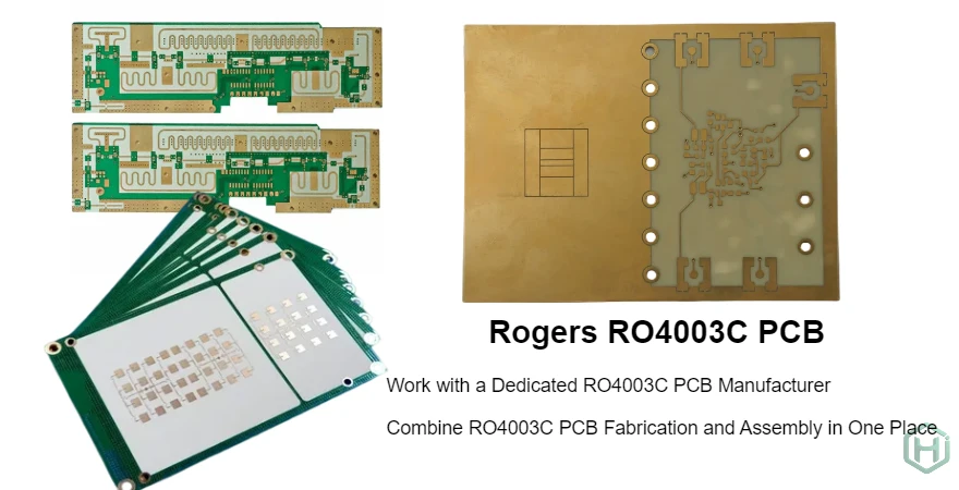
When RF, microwave and high-speed digital designs move beyond the limits of standard FR-4, Rogers RO4003C quickly becomes one of the most practical laminate options. To get the performance promised in the datasheet onto real hardware, you need a RO4003C PCB manufacturer that understands both the material and the production process.
HILPCB is a PCB manufacturing and PCB assembly factory focused on high-frequency PCBs and mixed-signal boards. We build RO4003C high frequency PCBs for RF front-ends, filters, radar modules, antennas and high-speed interfaces, from prototype to series production.
RO4003C PCB Manufacturing for Real RF and Microwave Projects
Rogers RO4003C is a hydrocarbon/ceramic laminate designed for stable electrical performance over a wide frequency range. Compared with general FR-4, it offers:
- Controlled dielectric constant (Dk ≈ 3.38 in typical RF test conditions)
- Low loss tangent for reduced insertion loss at GHz frequencies
- Good dimensional stability and z-axis CTE for via reliability
- Predictable behavior for controlled-impedance transmission lines
As a dedicated RO4003C PCB manufacturer, HILPCB supplies boards and assemblies for applications such as:
- Power amplifier (PA) and low-noise amplifier (LNA) modules
- 2.4 GHz / 5 GHz / sub-6 GHz RF front-ends for Wi-Fi, 5G and IoT
- Microstrip and GCPW filters, couplers, splitters and baluns
- 24 GHz and 77 GHz radar and industrial sensing hardware
- Mixed-signal and high-speed digital platforms using RO4003C hybrid PCBs with FR-4
In many of these designs, RO4003C is used only in the RF or high-speed sections, while FR-4 carries control logic and power. Our role is to make this mixed environment stable and repeatable in production, often in combination with other RF substrates such as Rogers PCBs and Teflon PCBs, depending on the requirements of the overall system.
RO4003C PCB Stackup and Impedance Control in Production (Technical Focus)
For RF and high-speed designs, the PCB stackup is part of the circuit. As a RO4003C high frequency PCB manufacturer, HILPCB puts most of the engineering effort into stackup definition, impedance control and loss management.
Transmission Line Structures on RO4003C
We routinely manufacture RO4003C PCBs with:
- Microstrip lines on outer layers for antennas and matching networks
- Stripline structures inside multilayer PCBs for shielded high-speed channels
- Grounded coplanar waveguide (GCPW) for better isolation and compact RF routing
- Differential pairs and coupled lines for filters and high-speed serial links
For each structure, the finished geometry is aligned with your impedance targets, for example:
- 50 Ω single-ended microstrip or GCPW
- 75 Ω lines for specific RF standards
- 90–100 Ω differential pairs for high-speed digital interfaces
When you provide Gerber/ODB++ data and basic impedance requirements, we calculate appropriate line width and spacing based on:
- RO4003C core thickness and Dk
- Copper thickness including plating
- Solder mask coverage (open or covered RF traces)
This is the basis for consistent RO4003C RF PCB behavior from lot to lot.
Etch Compensation and Dimensional Tolerances
Impedance is sensitive to small dimensional changes. To keep it under control, HILPCB:
- Applies etch compensation so the finished line width matches the electrical target, not only the CAD drawing
- Uses stable etch processes with defined line/space capabilities (typically 3/3 mil, tighter on request)
- Monitors critical dimensions during production to keep variation within the impedance window
For customers who need direct verification, we can add impedance coupons on the RO4003C panel and perform TDR or impedance tests according to your specification.
Copper Roughness and Insertion Loss
At multi-GHz frequencies, conductor loss and copper surface profile become important. In RO4003C PCB fabrication, we pay attention to:
- Selecting suitable copper foils and treatments compatible with RO4003C laminates
- Keeping etch profiles and line edges clean to avoid excessive roughness and neck-downs
- Maintaining consistent process parameters so insertion loss remains stable between batches
For long RF paths and high-frequency filters, this helps maintain the low-loss characteristics expected from a Rogers RO4003C PCB.
Vias, Grounding and Thermal Paths
Vias on RO4003C boards are part of the RF and thermal design:
- Signal vias between RF layers are drilled and plated with parameters tuned for ceramic-filled materials to maintain via quality and reliability.
- Ground via fences and stitching vias around GCPW lines, cavities and shielding walls provide controlled return paths and isolation.
- Thermal vias under power devices create efficient heat paths into copper planes or metal back structures, which is crucial for PA and radar front-end designs.
As a RO4003C RF PCB manufacturer, we combine drilling, plating and layout rules to support both RF performance and long-term reliability.
Hybrid RO4003C + FR-4 Stackups
Many customers choose RO4003C hybrid PCBs where:
- RO4003C is used on RF layers and critical high-speed layers
- FR-4 is used for low-speed logic and power distribution to reduce cost
HILPCB supports this architecture by:
- Designing lamination sequences that respect the different CTE and mechanical behavior of RO4003C and FR-4
- Selecting appropriate bonding materials and press cycles
- Controlling panel warpage and layer registration for stable assembly and connector positioning
This allows you to keep RO4003C exactly where it brings value, while the rest of the system remains on cost-effective FR-4.
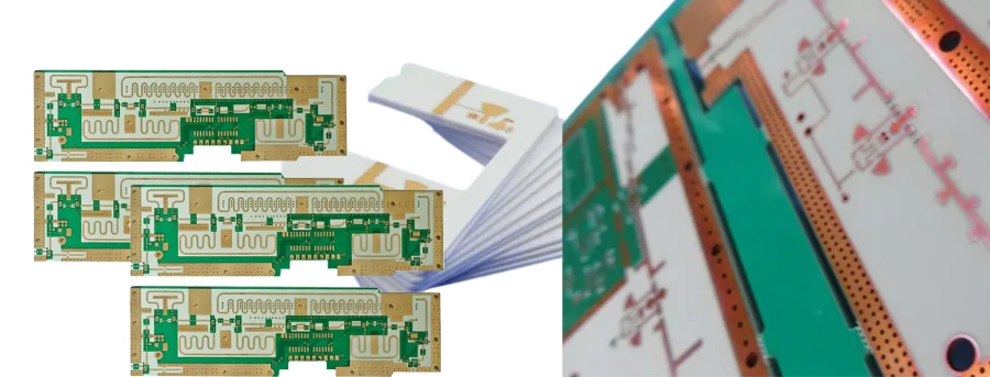
RO4003C PCB Manufacturing Capabilities at HILPCB
HILPCB offers a full range of RO4003C PCB manufacturing options for prototype and production:
- Layer count: 2–20+ layers for RO4003C PCBs; higher layer counts in hybrid RO4003C/FR-4 constructions.
- Finished thickness: common builds around 0.8 mm, 1.0 mm, 1.6 mm and custom thickness using RO4003C cores and prepregs.
- Copper weight: 0.5 oz, 1 oz, 2 oz; localized heavy copper available for high-current or high-power sections.
- Minimum line/space: typically 3/3 mil; finer features evaluated case by case.
- Minimum drill size: mechanical drills down to 0.2 mm; laser-drilled microvias in suitable stacks.
- Surface finishes: ENIG, immersion silver, OSP and others according to RF and assembly requirements.
- Testing: 100% electrical test; optional impedance coupons and additional RF test structures on request.
These capabilities allow HILPCB to act as your RO4003C PCB manufacturer from engineering samples to stable serial production, and integrate smoothly with our small-batch assembly services during development and large-volume assembly for mature products.
RO4003C PCB Assembly and Module Build
HILPCB is not only a board shop. We also provide RO4003C PCB assembly (PCBA) for RF and high-speed designs, so you can move from layout to test-ready hardware in a single factory.
Our RO4003C PCBA services include:
- SMT assembly for RF ICs, MMICs, QFNs, BGAs and discrete components
- Mounting of RF connectors such as SMA, SMP, edge-launch and board-to-board connectors
- Soldering of shield cans and mechanical frames for RF isolation
- Reflow profiles tuned for RO4003C and hybrid RO4003C/FR-4 stacks
- AOI and X-ray inspection, plus cooperation on functional test procedures if required
By combining RO4003C PCB fabrication and assembly under one roof, HILPCB helps reduce handling steps, shorten lead time and simplify communication during development and ramp-up. For projects that require integration beyond the PCB level, we can extend the scope to box-build assembly and full turnkey assembly, delivering complete electronic units based on your RO4003C designs.
Typical Use Cases for HILPCB RO4003C PCBs
With combined manufacturing and assembly, HILPCB supports a broad range of RO4003C high frequency PCB applications, for example:
- WLAN and IoT RF front-end modules in the 2.4 GHz and 5 GHz bands
- Sub-6 GHz 5G small-cell radios and microwave backhaul equipment
- X-band, Ku-band and other microwave point-to-point links
- 24 GHz and 77 GHz radar front-ends for automotive and industrial sensing
- Mixed-signal platforms where high-speed digital and RF circuits share the same assembly
In each case, the same RO4003C PCB manufacturer and assembler is responsible for stackup, impedance, loss and assembly quality.
Information to Prepare for a RO4003C PCB Project with HILPCB
To start a project with HILPCB as your RO4003C PCB manufacturer, the following information is helpful:
- Gerber, ODB++ or IPC-2581 design data (you can quickly check the data before sending using our online Gerber viewer and PCB viewer)
- Target layer count and expected quantities (prototype, small batch, mass production)
- Indication of which layers require RO4003C and whether a hybrid RO4003C + FR-4 stack is needed
- Key impedance requirements and main operating frequency bands
- Assembly requirements: BOM, pick-and-place files and any special notes for RF components and connectors
With these details, our engineering team can propose a practical build plan, lead time and testing options for your RO4003C RF PCBs and complete assemblies.
By specializing in HDI PCBs, high-frequency PCBs, and hybrid stackups, HILPCB provides a seamless transition from RF layout and high-speed design to stable, repeatable hardware. If your next project requires a reliable PCB manufacturer capable of handling both advanced RF and HDI PCB manufacturing, as well as assembly, HILPCB is ready to support you from prototype through to production.
Common Questions
What makes RO4003C a common choice for RF PCB projects?
RO4003C offers stable dielectric performance, relatively low loss, and processing behavior that is familiar to many PCB manufacturers. That combination makes it attractive for microwave, RF front-end, and mixed-signal designs that need better performance than standard FR-4.
Can RO4003C be combined with FR-4 in the same stack-up?
Yes, hybrid stack-ups are common when only selected RF layers need low-loss material. The key challenge is controlling lamination, registration, and thermal-mechanical compatibility between the RO4003C and FR-4 sections.
What project details should be shared before requesting a RO4003C quotation?
It helps to provide target frequency bands, layer count, impedance requirements, quantity stage, and whether assembly is needed. Those details let the manufacturer recommend a practical build plan instead of quoting only the base laminate.
Is assembly support important for RO4003C boards?
In many RF products, yes. Connector mounting, shield structures, fine-pitch RF devices, and mixed-material stack-ups all benefit from assembly processes that are tuned to the board construction and final use case.