
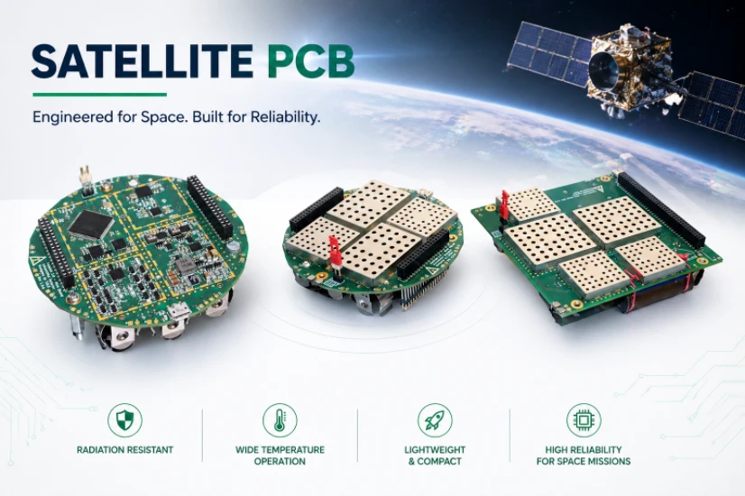
Building electronics for orbit means accepting constraints that terrestrial designers never face. No convective cooling — heat leaves the board only through radiation to cold space and conduction through mounting hardware to the spacecraft's thermal bus. Charged particles from solar proton events and trapped radiation belts upset flip-flops, latch up CMOS circuits, and gradually degrade insulation resistance over mission lifetimes of 7–18 years. Volatile compounds outgassing from PCB materials in vacuum deposit molecular contamination on optics, solar cells, and thermal control surfaces — permanently reducing their performance. And the ride to orbit subjects every board to 14 g RMS random vibration across 20–2,000 Hz for three minutes per axis, plus pyrotechnic separation shock exceeding 2,000 g.
The NewSpace revolution has added cost and schedule pressure on top of these technical constraints. A constellation operator ordering 500 identical processor boards for LEO satellites needs space-grade reliability at commercial lead times and pricing — not 18-month qualification cycles producing 10 boards at $50,000 each. For the wider system view, see our spacecraft PCB article.
HILPCB produces satellite PCBs to IPC-6012 Class 3 and Class 3/A on materials meeting NASA ASTM E595 outgassing requirements, with full raw-material-to-ship traceability. Our manufacturing supports up to 64 layers for complex satellite processor and payload boards, and production scales from single qualification units through constellation deployments.
Menu Navigation
- Material Requirements for Vacuum, Radiation, and Thermal Cycling
- IPC-6012 Class 3/A: Beyond Standard High-Reliability
- Thermal Design Without Convection
- Vibration and Launch Load Survivability
- CubeSat and NewSpace Pragmatic Qualification
- Conformal Coating and Surface Protection for Space
Material Requirements for Vacuum, Radiation, and Thermal Cycling
Space environments impose three simultaneous material challenges that don't exist in combination anywhere on Earth: hard vacuum, ionizing radiation, and extreme thermal cycling. Every polymer in the PCB stack-up — laminate resin, solder mask, legend ink, adhesive, conformal coating — must be individually qualified against all three.
Outgassing Qualification
NASA's ASTM E595 test measures total mass loss (TML ≤ 1.0%) and collected volatile condensable materials (CVCM ≤ 0.10%) when a material sample is heated to 125°C in vacuum for 24 hours. Most standard FR-4 laminates pass TML, but some solder mask formulations — particularly UV-cured types with residual photoinitiator — fail CVCM. Legend inks and adhesives are frequent failure points. HILPCB maintains a qualified materials list (QML) of laminates, solder masks, legend inks, and adhesives that have passed ASTM E595 testing with certificates from accredited laboratories. Using pre-qualified materials eliminates 4–8 weeks of material testing from the program schedule.
Radiation Effects on PCB Materials
Total ionizing dose (TID) degrades polymer insulation resistance and dielectric strength through chain scission and free radical formation. Standard FR-4 epoxy systems maintain acceptable properties to approximately 10 krad(Si) — adequate for LEO missions with moderate shielding. Polyimide-based materials (used in flex and rigid-flex space circuits) tolerate 50–100 krad. For missions in high-radiation environments — MEO navigation constellations, GEO communications, or Jupiter-bound probes exceeding 100 krad — ceramic substrates, radiation-hardened laminates, or additional shielding mass must be considered. Board-level mitigation for these environments is covered in our radiation hardened PCB guide.
Thermal Cycling Endurance
LEO satellites experience 15–16 eclipse/sunlit cycles per day. External-mounted PCBs see temperature swings from -65°C (eclipse) to +120°C (direct solar illumination), while internally-mounted boards cycle -20°C to +60°C. Over a 7-year LEO mission: 40,000+ thermal cycles. Via barrel cracking from cumulative z-axis CTE stress is the primary failure mode. High-Tg laminates (Tg ≥ 170°C, z-axis CTE ≤ 3.0% from 50–260°C) with copper-filled vias reduce this risk. HILPCB performs thermal cycling qualification on coupon-level test vehicles — representative via structures cycled through the mission profile — before committing flight panel fabrication. Cycle-life data specific to the customer's stack-up and via design is provided as part of the qualification package.
IPC-6012 Class 3/A: Beyond Standard High-Reliability
IPC-6012 Class 3 represents high-reliability fabrication for military and medical applications. Class 3/A (Addendum for Space and Military Avionics Applications) adds requirements specifically addressing the space environment's unique failure modes.
What Changes in Class 3/A
- Via Barrel Plating Minimum: 25 µm (1.0 mil) versus 20 µm (0.8 mil) for standard Class 3. This 25% increase in barrel thickness provides additional margin against cracking from thermal cycling and vibration-induced board flexure. HILPCB's plating process targets 30 µm nominal to provide margin above the minimum.
- Microsection Analysis Depth: Every production lot includes microsection analysis of qualification coupons containing via structures representative of the flight board design — through-hole, blind, buried, and micro-vias. Acceptance criteria for barrel thickness, etchback, resin smear, inner-layer connection quality, and plating voiding are tighter than Class 3.
- Conductor Dimension Control: Tighter tolerance on trace width and spacing — reduced acceptance for undercutting and over-etching that weakens conductors or reduces isolation distances. Critical for fine-pitch BGA breakout patterns on satellite processor boards (0.8 mm pitch packages with HDI micro-via escape routing).
- 100% Electrical Testing: No statistical sampling — every board undergoes continuity and isolation testing. Ionic cleanliness below 1.0 µg NaCl/cm² (versus 1.56 µg for standard Class 3). Surface insulation resistance (SIR) testing on representative comb patterns validates that contamination levels won't cause electrochemical migration under the sustained voltage bias and thermal cycling conditions of space operation.
- Documentation and Traceability: Full material lot traceability, process parameter records (lamination temperature/pressure profiles, plating bath chemistry logs, drill parameters), and deviation reports retained for the mission lifetime plus contractual retention periods (typically 20+ years for GEO missions). HILPCB's MES system maintains this traceability digitally with secure archived backups.
Thermal Design Without Convection
In orbit, conduction and radiation are the only heat transfer mechanisms available. The PCB's thermal design must create efficient conduction paths from heat-generating components to the board's mounting interface, where thermal straps or hardware connect to the satellite's thermal control system.
Board-Level Thermal Strategies
- Internal Copper Plane Heat Spreading: Continuous 2+ oz copper planes on multilayer PCBs spread heat laterally from processor and FPGA hotspots toward the board's mounting edges. The thermal conductivity of copper (390 W/m·K) versus FR-4 substrate (0.3 W/m·K) means virtually all lateral heat flow occurs through the copper planes. Plane continuity under and around hot components is critical — slots, splits, or via-free zones in the plane create thermal bottlenecks.
- Thermal Via Arrays: Dense via arrays connect top-side component thermal pads to internal planes and the board's bottom surface. Copper-filled vias at 0.3 mm drill on 1.0 mm pitch provide the lowest thermal resistance — approximately 10–15 °C/W through a 1.6 mm board for a typical 100-via array. Open (unfilled) vias have 2–3× higher thermal resistance.
- Copper Coin Inserts: For conduction-cooled chassis-mounted boards (common in GEO satellite transponders and military space payloads), HILPCB presses machined copper coins into board cavities — thermal resistance below 1 °C/W from the component surface through the board to the chassis interface. Available on boards up to 64 layers.
- Component Derating: Space programs typically derate power dissipation to 60–80% of rated values. Thermal analysis assumes worst-case solar illumination, worst-case attitude, and end-of-life thermal control surface degradation. The PCB's thermal design must accommodate this conservatism — providing margin that seems excessive by terrestrial standards but is necessary for missions where repair is impossible.
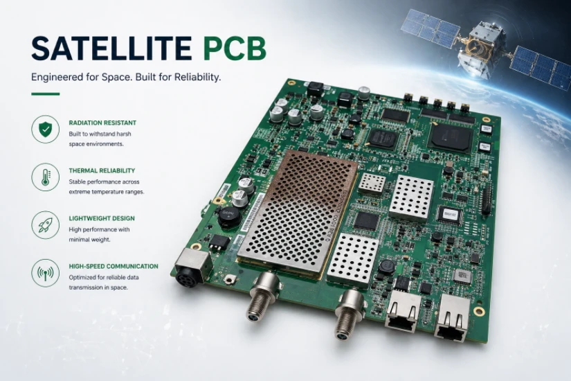
Vibration and Launch Load Survivability
Launch environments per GSFC-STD-7000 (NASA) or ECSS-E-ST-10-03 (ESA) typically specify 14 g RMS random vibration across 20–2,000 Hz for 2–3 minutes per axis. Pyrotechnic separation events generate shock spectra reaching 1,000–3,000 g at frequencies above 1 kHz. How boards are qualified against these loads is covered in space testing PCB requirements.
Board-Level Vibration Engineering
- Resonance Management: The board's fundamental resonant frequency must be above the launch vehicle's primary excitation frequency — typically above 100–200 Hz for small satellite boards. Adding intermediate mounting points, stiffening ribs, or constraining the board's unsupported span shifts the resonance upward. A 150 × 100 mm board with four corner mounts has a lower fundamental frequency than the same board with an additional center mount — the center mount can increase the first resonant frequency by 2–3×.
- Solder Joint Reliability Under Vibration: BGA packages experience higher cyclic stress under vibration than leaded packages due to the rigid underfill-free connection. Corner balls see the highest strain — strain proportional to the DNP (distance from neutral point, i.e., package center). For large BGAs (>25 mm), underfill adhesive between the package and PCB distributes stress across the entire array, improving vibration fatigue life by 5–10×.
- Component Staking: Tall, heavy components — electrolytic capacitors, inductors, transformers, connectors, relays — are most susceptible to mechanical failure under vibration and shock. Staking adhesive (UV-curable acrylate or two-part epoxy) applied at component bodies anchors them to the PCB surface, transferring vibrational loads from the solder joints to the adhesive bond. HILPCB applies staking per customer-specified maps with optical inspection of coverage and fillet formation.
- Board Fabrication Quality Contributions: Consistent board thickness (±10% of nominal) prevents resonance prediction errors — a board that's 10% thinner than expected has a proportionally lower stiffness, shifting its resonant frequency into the launch vehicle's excitation band. Via barrel integrity ensures vias don't crack under board flexure during vibration — confirmed by microsection analysis at qualification.
CubeSat and NewSpace Pragmatic Qualification
Traditional space programs spend 12–18 months qualifying a PCB design through progressive build-test-analyze cycles. NewSpace constellation programs need 500+ identical boards delivered in 8–12 weeks with reliability adequate for 5–7 year LEO missions — not the 18-year life of a GEO communications satellite.
Scaled Qualification Approach
- Class 3 with Space Materials: HILPCB offers IPC-6012 Class 3 fabrication using ASTM E595-qualified materials, 100% electrical testing, and lot-level microsection analysis — without the full Class 3/A documentation overhead. This provides space-grade materials and processes at commercial lead times (3–4 weeks for production quantities).
- Constellation Volume Economics: For programs ordering 200–5,000 boards, panel optimization, automated test fixture development, and SPC monitoring of critical parameters make high-reliability fabrication economically viable. Volume pricing for space-grade boards approaches commercial high-reliability pricing — 3–5× standard commercial, rather than the 10–20× typical of traditional space programs.
- Design for Qualification Integration: HILPCB's DFM review identifies potential qualification risks during the design phase — via aspect ratios approaching reliability limits, material stress points near Tg, copper balance issues causing panel warpage — before the first panel ships. This prevents qualification surprises that delay constellation deployment schedules.
- Heritage and Lot Continuity: Once a board design passes flight qualification, maintaining identical materials, processes, and parameters across production lots is critical. HILPCB's MES system locks process parameters after qualification approval — any deviation triggers formal change notification to the customer before proceeding.
Conformal Coating and Surface Protection for Space
Space-Grade Coatings
- Parylene C: Vapor-deposited at room temperature, producing uniform, pinhole-free coverage (5–25 µm) even over sharp component edges, under low-profile chips, and into narrow gaps that liquid coatings can't reach. Prevents tin whisker growth (critical for pure tin component terminations), reduces corona discharge risk at high-voltage traces in partial vacuum, and provides contamination barrier during ground handling and integration. Outgassing properties: TML = 0.5%, CVCM = 0.02% — well within ASTM E595 limits.
- Parylene HT: Extended temperature rating to +350°C for boards mounted near thruster plumes, solar concentrators, or other high-temperature zones. Similar deposition process to Parylene C but with fluorinated chemistry providing improved UV stability for external-facing surfaces.
- Acrylic Coatings (IPC-CC-830 Type AR): Lower cost and easier rework than parylene — critical during satellite integration and test phases when wire additions, component replacements, and jumper modifications are common. Acrylic coatings have higher outgassing than parylene — post-coating bake at 125°C for 24 hours typically brings TML/CVCM within ASTM E595 limits but must be verified for each specific coating product.
- Selective Coating Requirements: Connector pins, test points, RF connectors, and thermal interface surfaces must remain uncoated. Masking strategy — liquid masking compound, polyimide tape, or custom silicone plugs — defined before coating application. HILPCB coordinates selective coating with qualified coating vendors, providing component height maps and keep-out zone definitions.
Begin your satellite PCB program with a materials and qualification strategy review →
Frequently Asked Questions
What does ASTM E595 outgassing compliance mean for satellite PCBs? In the vacuum of space, volatile compounds in standard PCB materials can outgas and condense on sensitive optics and solar panels, degrading their performance. ASTM E595 testing ensures that laminates, soldermasks, and coatings meet strict Total Mass Loss (TML ≤ 1.0%) and Collected Volatile Condensable Materials (CVCM ≤ 0.10%) limits.
How do satellite PCBs dissipate heat without air convection? Without air, heat can only be removed via conduction and radiation. Space-grade PCBs use continuous heavy copper internal planes and dense copper-filled thermal via arrays to spread heat laterally to the board's mounting edges, where it conducts into the spacecraft's thermal chassis.
Why is IPC-6012 Class 3/A required for space electronics? IPC-6012 Class 3/A adds stringent requirements specifically for space and military avionics, such as increasing the minimum via barrel plating thickness to 25 µm (1.0 mil). This extra plating provides crucial margin against via cracking caused by severe vibration during launch and extreme thermal cycling in orbit.
What conformal coatings are best for space environments? Parylene C is highly recommended because it is vapor-deposited, creating a uniform, pinhole-free layer that prevents tin whiskers and reduces corona discharge risk in partial vacuum, all while easily passing NASA outgassing requirements.