
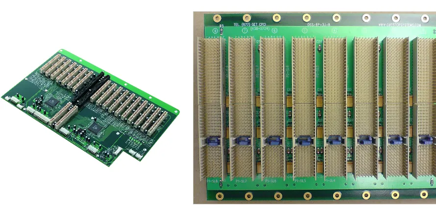
A server backplane PCB is the interconnect board that routes defined signal, power, management, and control paths between replaceable server, storage, switch, or accelerator modules. It does not make a channel compliant by itself: the usable link includes packages, daughtercards, connectors, vias, backplane traces, cables or retimers where present, and the endpoint.
This guide turns that complete path into a manufacturable and verifiable release package.
Key Takeaways
- Assign one owner to the complete channel from transmitter package to receiver package; do not optimize the backplane in isolation.
- Choose classic backplane, midplane, orthogonal, or cabled architecture from reach, cooling, service, mechanics, connector count, and validation constraints—not from a universal rule.
- Allocate insertion loss, return loss, crosstalk, skew, discontinuity, and test access before layout. A nominal impedance value alone is not a channel budget.
- Select laminate, stackup, via treatment, and connector footprint from the project loss model. Material brands and fixed layer counts are not specifications.
- Control press-fit holes with the connector manufacturer's application specification, finished-hole data, plating evidence, tooling, insertion-force limits, and first-article inspection.
- Keep fabrication coupons, connector qualification, assembled-channel measurements, and PCIe/CXL/system compliance as separate evidence layers.
- Send the fabricator a complete stackup, drill/backdrill package, connector controls, coupon plan, dimensions, tolerances, and acceptance matrix with the RFQ.
Table of Contents
- What does a server backplane actually own?
- Which backplane architecture fits the system?
- Build an end-to-end channel ownership map
- Allocate the signal-integrity budget before layout
- Choose materials and stackup from measured needs
- Control vias, backdrill, and connector transitions
- How should press-fit connector zones be released?
- Separate power, thermal, and airflow responsibilities
- Manufacturing evidence matrix
- Validation ladder from coupon to system compliance
- Common failure modes and corrective actions
- Cost and schedule drivers
- Server backplane PCB RFQ checklist
- Reference standards and responsibility boundaries
- What can HILPCB support?
- Frequently asked questions
What Does a Server Backplane Actually Own?
The backplane owns only the functions assigned to it. A storage backplane may fan out PCIe lanes and management buses. A compute chassis backplane may connect modular trays, distribute auxiliary power, and carry clocks or sideband signals. A switch chassis may instead use orthogonal connectors or high-speed cables.
The backplane is therefore not automatically the server's “main board.” CPU and GPU packages, memory interfaces, local voltage regulators, and high-frequency decoupling commonly remain on motherboards or accelerator cards. If the backplane distributes high current, its job is to meet the voltage-drop, temperature, connector, protection, and fault requirements of those distribution paths. It does not replace load-point transient design on the consuming module.
This boundary stops teams from assigning CPU/GPU transient performance to a remote board and keeps attention on long channels and repeated connector/via transitions.
Which Backplane Architecture Fits the System?
"Backplane" and "midplane" describe layout families, not guaranteed insertion directions or cooling outcomes. The chassis, connectors, card orientation, power, cooling, and service model determine the implementation.
| Architecture | Typical arrangement | Strong reason to choose it | Main engineering burden | Evidence to request early |
|---|---|---|---|---|
| Classic backplane | Plug-in cards connect through a shared board; cards may be serviced from one or more chassis zones | Simple modular interconnect and centralized distribution | Long traces, dense connector fields, board size, press-fit and backdrill control | Chassis drawing, connector map, route-length study, dimensional tolerance stack |
| Midplane | Modules or connector systems interface through a central board from different chassis regions | Front/rear functional partition or shorter paths for a specific mechanical concept | Access from both sides, connector alignment, obstruction and service sequence | Mechanical datum scheme, airflow model, mating sequence and insertion tooling |
| Orthogonal/direct orthogonal | Connector systems join cards in perpendicular orientations, sometimes minimizing routed distance on an intermediate board | Reduce some long board routes or enable dense switch fabrics | Connector escape, mechanical stack, skew between equivalent paths, test access | Connector models, card-to-card tolerance analysis and full transition simulation |
| Cabled backplane or cable-assisted fabric | High-speed cable assemblies carry selected lanes while a PCB handles lower-speed, power, or connector organization | Extend reach or bypass a lossy long PCB segment | Cable/connector discontinuities, assembly routing, bend/service constraints and added interfaces | Cable S-parameters, routing envelope, mating-cycle requirements and assembled-channel plan |
No architecture is automatically best for airflow. Treat pressure drop and inlet-temperature uniformity as system measurements, not as labels attached to board type.
Build an End-to-End Channel Ownership Map
The key design document is a channel ownership map naming every segment, model owner, limits, and handoff evidence.
ASIC/package → host or daughtercard → connector → backplane → connector → endpoint card/package
Add cables, retimers, switches, test fixtures, and extra connector pairs wherever used. An omitted block becomes an unbudgeted discontinuity.
| Channel segment | Primary owner | Input required before layout freeze | Evidence at release |
|---|---|---|---|
| Transmitter/receiver package | Silicon or package supplier; system SI owner | Package model, launch definition, reference plane and protocol conditions | Model revision and correlation status |
| Host/daughtercard route | Card designer | Stackup, trace/via model, breakout constraints and connector launch | Routed topology, extraction/model report and coupon plan |
| Connector pair | Connector supplier with system mechanical owner | Mated models, footprint, anti-pad, finished-hole range, stack and application specification | Approved part/revision, qualification boundary and assembly instructions |
| Backplane route | System SI owner and PCB designer; fabricator owns contracted construction | Loss/skew budget, stackup, material and copper inputs, via/backdrill definition, spacing rules | Released artwork plus correlated fabrication evidence |
| Cable or retimer, if used | Component supplier and system owner | Models, equalization/latency constraints, power/management requirements | Approved configuration and subsystem test result |
| Complete assembled channel | System owner | Reference planes, fixtures, measurement method, de-embedding and pass limits | TDR/VNA or protocol-specific channel data plus system test |
The fabricator provides manufacturability and construction evidence, not package behavior, connector qualification, receiver settings, firmware, or unspecified compliance.
Allocate the Signal-Integrity Budget Before Layout
Start with the applicable protocol, form factor, connector, topology, and data rate. PCIe, CXL, Ethernet, and proprietary SerDes links require their selected revision and channel limits. Do not mix a generic connector data-rate claim with a different lane, modulation, reach, fixture, or compliance method.
Allocate at least these items by segment:
- insertion loss across frequency, including dielectric, conductor, via, connector, and cable contributions;
- return loss and impedance discontinuity at launches, vias, anti-pads, connectors, and layer transitions;
- near-end and far-end crosstalk from routing, connector pin fields, and breakout regions;
- differential skew from route geometry, glass-weave interaction, connector asymmetry, layer changes, and package escape;
- differential-to-common-mode conversion where symmetry is disturbed;
- jitter/noise or a protocol-specific channel metric such as COM when the applicable method requires it;
- measurement and model uncertainty, manufacturing tolerance, temperature, and aging margin;
- test access, fixture loss, calibration plane, de-embedding method, and sample plan.
A nominal differential impedance may be specified, but its target and tolerance come from the selected interface. A passing impedance coupon does not prove loss, crosstalk, or the assembled connector transition.
Use electromagnetic models where discontinuities dominate. Dense connector fields, backdrilled vias, breakout cavities, and orthogonal transitions require their actual three-dimensional structures and materials.
Choose Materials and Stackup From Measured Needs
Material brands and "20-plus layers" are not requirements. The construction must close channel, mechanical, fabrication, availability, and cost budgets with documented margin.
Build a material selection table using:
| Input | Why it matters | Procurement/release question |
|---|---|---|
| Dk and Df with test method and frequency | Published values vary by method and may not equal the design value used by the field solver | Which value, method, frequency, resin content, and tolerance will be used for modeling and impedance? |
| Copper profile/roughness | Conductor loss can become material at high frequency and depends on the foil-treatment interface | Which foil option is available on each signal layer, and is its model included? |
| Glass style and resin content | Affect thickness, Dk distribution, skew risk, fill, and dimensional behavior | Are spread-glass or alternate constructions needed on critical layers, and can the supplier hold them? |
| Tg, decomposition behavior, Z-axis expansion, and moisture performance | Affect lamination, drilling, assembly, and reliability; Tg alone does not rank high-speed performance | What thermal and reliability envelope does the product require? |
| Thickness tolerance and availability | Move impedance, loss, finished thickness, connector engagement, and schedule | Are production lots and alternates controlled before qualification? |
| Hybrid-material compatibility | Different resin systems can change lamination, registration, adhesion, and requalification burden | Has the exact hybrid construction been reviewed and proven by the selected fabricator? |
Balance copper and dielectric construction where practical. Coordinate resin flow, plane coverage, drill aspect ratios, lamination, thickness, and bow/twist. Large boards also require early control of registration, scale compensation, connector position, and flatness.
Selective low-loss layers can reduce cost only when the hybrid construction preserves the channel and is producible consistently.
Control Vias, Backdrill, and Connector Transitions
For every critical lane, record start/end layers, unused plated section, reference vias, anti-pad, connector launch, and shared test pads. Model that transition with the selected stackup.
Backdrilling removes a defined unused via segment; it is not a universal high-speed requirement. A complete backdrill release includes:
- source and destination side, start layer, stop layer, and all affected drill IDs;
- primary plated-hole diameter, backdrill diameter, clearance to adjacent copper, and breakout rules;
- target residual stub or depth condition with tolerance derived from the electrical model and layer registration capability;
- restrictions around connector press-fit zones, nonfunctional pads, test pads, and shared structures;
- depth-verification method, coupon/witness structure, sampling plan, and acceptance evidence;
- change-control rule for stackup, drill compensation, laminate lot, or fabricator process changes.
The residual structure, board construction, drilling method, registration, and inspection approach must agree; do not copy a generic supplier tolerance.
Likewise, "3W" is only a heuristic. Crosstalk depends on stackup, coupling length, aggressors, connector pinout, breakout, and frequency content; use the project budget and extraction.
How Should Press-Fit Connector Zones Be Released?
Press-fit reliability couples connector geometry, finished holes, plating, board thickness, tooling, support, insertion force, and inspection. Start from the connector manufacturer's current application specification, not a copied hole tolerance.
The connector-zone drawing should define:
- approved connector manufacturer and exact part/revision;
- nominal drill, finished-hole range, plating system, copper thickness requirement, and any surface-finish restrictions from the application specification;
- board thickness and local stack condition that affects compliant-pin engagement;
- hole pattern, true position, datum scheme, connector keep-outs, and mating alignment features;
- allowable rework or replacement method and the maximum permitted insertion/removal history;
- press tooling, board support, insertion direction, force/displacement monitoring, and stop condition;
- inspection and qualification sample plan, including hole measurement, microsection or other agreed evidence, connector seating, damage review, and electrical checks.
For large arrays, verify the press, fixture, board support/deflection, component clearance, and coplanarity as one system. Provide the connector supplier's tooling and process instructions with the build package.
Surface finish is application-dependent. Separate press-fit holes, soldered features, edge contacts, test pads, and storage controls; ENIG or ENEPIG is not an automatic requirement.
Separate Power, Thermal, and Airflow Responsibilities
A backplane may distribute bulk or auxiliary power and management rails. Design each path from current, drop, contact resistance, fault energy, protection, temperature, and mechanical interfaces. Copper weight alone does not prove capacity.
Budget connector contacts, vias, planes, protection, busbars/fasteners, and returns. Measure drop and temperature at worst-case current and cooling. The consuming module still owns local regulation and high-frequency decoupling unless explicitly reassigned.
State inlet temperature, airflow/pressure, blockage, neighboring modules, allowed temperatures, and fan-fault behavior. The chassis team owns system cooling validation.
Manufacturing Evidence Matrix
Name the evidence for each risk instead of asking for “full inspection.”
| Risk | Fabrication/assembly control | Evidence to retain | What it does not prove |
|---|---|---|---|
| Material identity and construction | Approved laminate/foil list, stackup traveler, controlled alternates | Certificate/lot traceability if required, stackup record and material data | Whole-channel performance |
| Impedance | Controlled geometry and project coupon | TDR result with coupon design, limits, equipment and lot link | Connector launch, loss, crosstalk or system compliance |
| Insertion loss/material correlation | Loss coupon or agreed characterization vehicle when required | S-parameter or agreed loss result with method and frequency range | Assembled channel without connectors/cards |
| Layer registration and dimensional stability | Scale compensation, tooling strategy and panel controls | Registration coupon, microsection/tooling data, critical dimension report | Connector mating under chassis tolerance stack |
| Backdrill | Released map, diameter/clearance and controlled depth process | Coupon/witness or agreed cross-section/depth evidence tied to lot | Protocol compliance or receiver margin |
| Press-fit holes | Controlled drill/plating/final-hole process and connector application limits | Finished-hole data, plating/microsection evidence and sampling record | Connector supplier qualification or assembled insertion quality |
| Connector installation | Approved tooling, support, seating and force/displacement process | First-article installation record and agreed inspection/electrical data | Lifetime mating-cycle performance unless qualified |
| Flatness and connector position | Balanced construction, controlled routing/profile and dimensional inspection | Bow/twist plus connector/datum measurement to drawing | Chassis alignment unless the chassis stack is included |
| Net integrity | Customer netlist and appropriate bare-board electrical test | Lot-linked electrical-test record | High-frequency channel quality |
| Assembly quality | Defined solder/press-fit route and inspection access | First article, profile/AOI/X-ray or other method as applicable | Functional or system qualification |
AOI, X-ray, flying probe, TDR, VNA, microsection, and functional test answer different questions; no single method substitutes for the rest.
Validation Ladder From Coupon to System Compliance
Use a staged ladder so that no passing result is promoted beyond its scope.
| Evidence layer | Question answered | Typical artifact | Release owner |
|---|---|---|---|
| 1. Design/model review | Does the proposed channel have modeled margin with tolerances? | Topology, stackup, extracted models, channel budget and review record | System SI/design authority |
| 2. Bare-board fabrication | Did the fabricator build the specified construction and coupons? | Stackup, impedance/loss coupon, microsection, backdrill and dimensional data | PCB fabricator against purchase drawing |
| 3. Connector/process qualification | Are connector, hole, tooling, insertion, and mechanical conditions qualified within their stated boundary? | Connector supplier qualification plus project assembly/first-article record | Connector supplier and system/assembly owner |
| 4. Assembled-channel measurement | Does the built path correlate with models and meet electrical limits? | Calibrated/de-embedded TDR or VNA data, fixtures and uncertainty statement | System SI/test owner |
| 5. Protocol and platform test | Does the implementation pass the applicable electrical/protocol test plan? | PCIe/CXL/other protocol test result and interoperability evidence | System owner and authorized test route |
| 6. Server/product release | Does the complete server meet thermal, EMC, safety, reliability, service, and platform requirements? | Product qualification and compliance file | OEM/product authority |
The PCB supplier can support contracted bare-board and assembly evidence, but not replace system protocol, interoperability, safety, EMC, or product release.
Common Failure Modes and Corrective Actions
| Failure pattern | Likely cause | Corrective action before the next build |
|---|---|---|
| Model passes, hardware margin collapses | Connector/via, roughness, fixture, or tolerance omitted | Reconcile channel map, models, coupons, and de-embedded measurements |
| Large lane-to-lane skew | Weave, layer, connector, or transition asymmetry | Compare physical constructions; revise weave/layer and transition symmetry |
| Return-loss peak at connector | Footprint, anti-pad, reference via, or stackup error | Co-design the launch with supplier model and 3D extraction |
| Wrong backdrill result | Ambiguous layers, clearance, tolerance, or drill map | Release explicit drill IDs and lot-linked depth evidence |
| Press-fit damage or poor seating | Hole/plating mismatch, support/tooling, deflection, or insertion error | Inspect holes, qualify fixture, and monitor force/displacement |
| Board fits drawing, not chassis | Datums, position, flatness, or system tolerances conflict | Share datums and perform tolerance plus first-fit checks |
| Hot connector or power path | Contact imbalance, constriction, return path, or cooling | Measure drop/temperature and revise current allocation |
| Coupon passes, protocol fails | Coupon covers only one construction attribute | Correlate the assembled channel and debug at protocol level |
Requalify affected evidence after material, stackup, connector, drill/backdrill, press-fit tooling, assembly-site, or channel-route changes.
Cost and Schedule Drivers
Cost follows construction and evidence, not layer count alone. Drivers include board/panel size, material, thickness, copper, lamination, drill/backdrill burden, connector position, press-fit tooling, coupons, dimensional sampling, electrical test, and yield risk.
The best cost reduction is requirements cleanup:
- remove unused lanes or connector positions after system review;
- shorten or cable difficult channels when the chassis trade study supports it;
- use the least complex stackup/via structure that meets the modeled budget;
- avoid unjustified tolerances and separate recurring lot evidence from one-time characterization.
Require quoted assumptions and exceptions; material substitutions or omitted evidence make bids non-comparable.
Server Backplane PCB RFQ Checklist
Design and fabrication files
- Gerber X2 or ODB++/IPC-2581 data as accepted by the supplier, plus NC drill and routed-profile data;
- fabrication drawing with outline, datums, connector locations, tolerances, bow/twist, and thickness;
- released stackup with layer names, copper, dielectric, material/foil requirements, controlled-impedance table, and allowed alternates;
- drill chart separating plated, non-plated, press-fit, slot, and backdrill operations, plus explicit backdrill layers/diameters/acceptance;
- netlist and revision-controlled readme resolving any file conflicts.
Channel and connector requirements
- protocol/version, topology, lanes/rate, connector/cable/retimer parts, and channel budget;
- connector manufacturer's current footprint and application specification;
- impedance/loss/skew/crosstalk limits and model assumptions, plus coupon drawings, sampling, methods, limits, and data format;
- press-fit finished-hole/plating limits, tooling, support, force/displacement, seating, inspection, and rework rules.
Product and process requirements
- quantities by stage, serialization/traceability, and applicable workmanship criteria with edition/addenda;
- environmental, thermal, shock/vibration, storage, cleanliness, finish, packaging, and shelf-life requirements;
- approved material/connector/component list and change-notification/requalification triggers;
- required first-article, microsection, impedance/loss, dimensional, electrical-test, press-fit, and assembly records;
- BOM, placement, special processes, programming, and functional-test specification if PCBA is included.
Supplier response required
- exact stackup and material proposal, modeled impedance geometries, and any deviations;
- panelization, drill/backdrill process, press-fit route, critical tolerances, inspection/sample plan, and evidence deliverables;
- exceptions, assumptions, alternates, qualification needs, schedule drivers, and requalification conditions;
- separate pricing for fabrication, coupons/data, connector installation, assembly, tooling, first article, and recurring production.
Reference Standards and Responsibility Boundaries
Applicable references may include:
- PCI-SIG PCI Express Base Specification and the applicable form-factor/compliance documents
- Compute Express Link Consortium CXL specification and compliance program for the selected version
- Open Compute Project MHS, DC-MHS, DC-SCM, or other platform specifications as applicable
- IEC 60352-5, solderless press-in connections
- IPC-2221 and IPC-2222, generic and rigid-board design requirements
- IPC-4101, base materials for rigid and multilayer printed boards
- IPC-6012 and IPC-A-600, rigid-board qualification/performance and acceptability
- IPC-TM-650 test methods used by the purchase specification
- J-STD-001 and IPC-A-610 when assembly workmanship is in scope
Use the exact editions, methods, classes, addenda, connector specifications, and customer drawings. A list does not create compliance.
The system owner controls architecture, channel limits, models, mechanics, cooling, firmware, interoperability, compliance, and product release. Fabricator and assembler own only contracted construction, processes, evidence, and change control.
What Can HILPCB Support?
Use HILPCB's backplane PCB manufacturing route for connector-heavy construction, drill/backdrill, stackup, and evidence review. Related high-speed PCB, multilayer PCB, and backplane design review pages provide supporting context.
Send the full package, identify the highest-risk channel/connector zones, and require confirmation of construction, deviations, coupons, dimensions, backdrill, press-fit scope, and evidence before treating any capability as committed. Submit it through the quote page.
Frequently Asked Questions
Is a server backplane always a high-layer-count PCB?
No. Layer count follows routing, reference planes, power, mechanics, and manufacturability. Large dimensions, press-fit fields, long channels, or connector position can make a lower-layer board difficult. Select the least complex stackup that meets the evidence-backed requirements.
Does a passing impedance coupon prove PCIe or CXL compliance?
No. It covers one transmission-line construction, not packages, all vias, connectors, cables, retimers, receiver settings, or system behavior. PCIe/CXL release needs the applicable assembled-channel, protocol, interoperability, and platform evidence.
Should every high-speed backplane use backdrilling?
No. Use it when the unused via consumes unacceptable margin and the drill geometry is manufacturable. Blind vias, layer changes, connector escape changes, or cables may be better. Decide from channel and tolerance analysis.
What is the most important press-fit PCB requirement?
There is no universal number. Align the connector application specification with finished holes, plating, thickness, position, tooling, support, insertion, seating, inspection, and rework as one qualified system.
What should be validated on the first server-backplane build?
Confirm construction, dimensions, connector fit, press-fit process, net integrity, coupons, backdrill evidence, and selected assembled-channel correlation. The first build does not prove full server compliance.
Conclusion
A reliable server backplane begins with ownership, not a material brand or layer count. Map the channel, choose the chassis architecture, allocate budgets, release connector/backdrill zones clearly, and require evidence that matches each risk. Keep coupons, connector qualification, assembled-channel measurement, and system release separate but connected.