
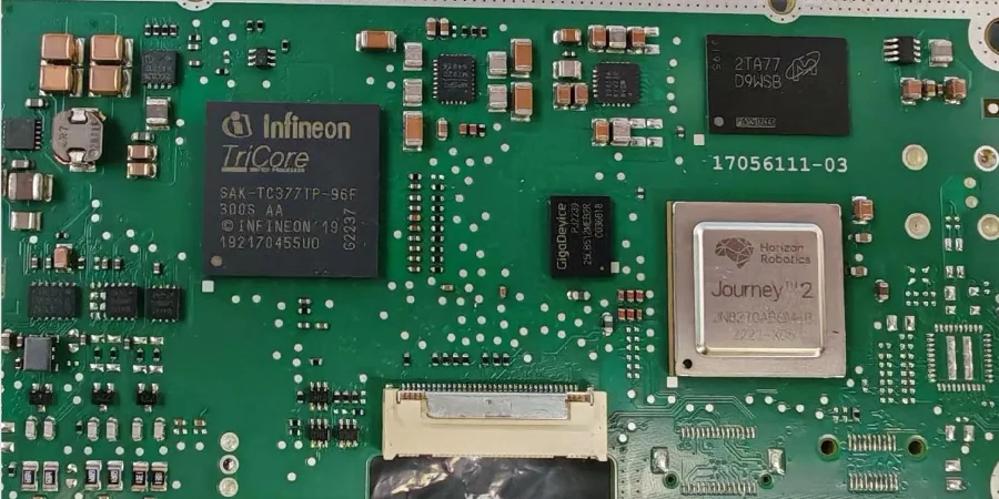
As the automotive industry accelerates toward electrification and intelligence, ADAS and EV power systems have become the core battleground of innovation. Their complexity, performance requirements, and safety-critical nature push unprecedented demands onto PCB design and assembly. In this environment, SMT assembly is no longer “just soldering”—it is a decisive factor for ECU functional safety, long-term reliability, and electromagnetic compatibility (EMC). From mmWave radar high-frequency signal integrity to high-voltage/high-current management in on-board chargers (OBC), every detail must meet automotive-grade standards.
From an automotive electronics engineer’s perspective, this article explains how precise SMT assembly plus advanced PCB design practices address ISO 26262 functional safety, AEC‑Q reliability expectations, and strict EMC regulations. We connect safety-architecture targets to production quality controls, showing how design principles become ASIL‑D-class hardware in real manufacturing.
Functional safety decomposition: ASIL targets, hardware metrics, and diagnostic coverage in SMT assembly
In automotive electronics, functional safety is the design foundation. ISO 26262 defines lifecycle safety requirements from concept through end-of-life, centered on allocating and achieving ASIL (Automotive Safety Integrity Level). For ADAS perception/decision units, or EV BMS and inverters, ASIL‑C or even ASIL‑D is common. That means hardware must be extremely reliable to avoid risk from random hardware failures.
SMT assembly quality directly impacts the probability of random hardware failures. A cold joint, an insufficient solder fillet, or a wrong placement can become a Single-Point Fault. To quantify hardware safety, ISO 26262 introduces three key hardware architectural metrics:
- SPFM (Single-Point Fault Metric): measures coverage of safety mechanisms for single-point faults. Target SPFM ≥ 99% (ASIL‑D). High-quality SMT assembly reduces single-point fault likelihood at the source by ensuring joint integrity and placement correctness.
- LFM (Latent Fault Metric): measures coverage of latent faults (multi-point faults not detected within a driving cycle). Target LFM ≥ 90% (ASIL‑D). For example, in redundant channels, if one channel component fails due to an assembly defect, diagnostic circuits must detect it—meaning the diagnostic circuits themselves must be assembled flawlessly.
- DC (Diagnostic Coverage): the percentage of specific component/function failures that safety mechanisms can detect. PCB test points and diagnostic nets require robust assembly to remain valid in real operation.
In practice, designs such as BMS balancing board impedance control directly affect accurate cell-voltage measurement, which is a functional-safety cornerstone for BMS. Any impedance deviation can lead to incorrect SOC/SOH estimation and create safety risk. Therefore, from PCB fabrication to assembly, trace width/spacing and dielectric behavior must be tightly controlled to ensure consistent impedance—one of the core strengths of specialized manufacturers like HILPCB.
High-density and high-frequency challenges: Microvia/stacked via in ADAS radar PCBs
ADAS systems—especially 77/79 GHz mmWave radar—place extremely strict demands on PCBs. High-frequency signals are highly sensitive to path length, impedance continuity, and parasitics. To fit RF front ends, high-speed processors, and power circuits into tight form factors, HDI becomes unavoidable.
In HDI designs, Microvia/stacked via technology is critical:
- Microvia: typically laser-drilled, with diameter < 150 µm, connecting adjacent layers. They shorten vertical signal paths and reduce parasitic L/C—key for high-frequency SI.
- Stacked Via: stacks multiple microvias to create vertical interconnect across many layers, increasing routing density and enabling shorter, more direct connections for high-pin-count BGAs.
However, Microvia/stacked via also raises new SMT assembly challenges. Ultra-small pads increase sensitivity to stencil printing accuracy, placement precision, and reflow profile control. Small deviations can cause defects such as solder balls, bridging, or opens. So successful ADAS radar PCB validation depends not only on RF design, but also on precision manufacturing and assembly capable of handling HDI. Validation must include strict S‑parameter testing (insertion loss, return loss) with network analyzers to prove performance. HILPCB’s HDI PCB manufacturing capability, combined with advanced assembly lines, helps ensure a clean handoff from design to physical hardware.
HILPCB automotive-grade HDI fabrication and assembly capability
- Fine-line capability: supports down to 2/2 mil (50/50 µm) trace/space to meet high-density BGA and RF design needs.
- Advanced via technology: supports Any-layer interconnect (Anylayer) and stacked microvia structures for extreme routing density.
- Precision assembly process: uses 3D SPI and 3D AOI to ensure solder quality on Microvia/stacked via pads.
- High-frequency material support: offers low-loss RF materials such as Rogers and Teflon to protect ADAS radar signal integrity.
- Strict validation workflow: supports full ADAS radar PCB validation, including impedance testing, TDR analysis, and reliability tests.
EV power PCB design: On-board charger PCB layout and high-voltage safety compliance
Unlike ADAS high-frequency/high-speed demands, EV power systems (OBC, DC‑DC converters, inverters) are dominated by high voltage, high current, and high heat. Their PCB design and assembly must prioritize electrical safety and thermal management.
A well-executed On-board charger PCB layout is the foundation of safety and performance. Key design considerations include:
- Creepage and clearance: strictly follow standards such as IEC 60664‑1, maintaining sufficient spacing between HV and LV domains and between different HV potentials to prevent arcing and leakage. This directly affects On-board charger PCB compliance.
- High-current paths: use thick copper (e.g., 3oz or thicker Heavy Copper PCB), busbars, or embedded copper to carry tens to hundreds of amps while minimizing voltage drop and heat.
- Thermal management: use dense Thermal Vias, copper pours, and tight heatsink coupling to move heat from power devices (MOSFET, IGBT) efficiently.
- Placement strategy: distribute hot parts to avoid hotspots; isolate high-voltage components from sensitive control nets to reduce coupling.
On-board charger PCB compliance is not only a design problem—it is tightly coupled to manufacturing and assembly. For example, laminate CTI (Comparative Tracking Index) must meet HV requirements. During SMT assembly, joints for HV capacitors and common-mode chokes must be well-formed and void-free to ensure long-term electrical reliability and mechanical strength. Any assembly defect can evolve into serious safety hazards under vibration or thermal cycling. Similarly, for BMS systems, precise BMS balancing board impedance control is critical for accurate sensing under high common-mode noise—requiring end-to-end impedance discipline from fabrication through assembly.
CISPR 25 / ISO 11452: EMC design and validation
EMC is another major automotive challenge. Dense in-vehicle electronics plus complex external electromagnetic environments mean any ECU can be either a noise source or a victim. The industry’s two primary standards are CISPR 25 (radiated emissions) and ISO 11452 (radiated immunity).
At the PCB level, EMC compliance requires a systematic strategy:
- Grounding: use solid multi-layer ground planes to provide low-impedance return paths for high-speed and noise currents. Partition analog ground, digital ground, and power ground appropriately with single-point connection rules.
- Filtering and shielding: at power inputs and I/O ports, use capacitors/inductors/ferrite beads to build π or T filters. Use metal shields over sensitive circuits (clocks, RF front ends) or strong emitters (switch-mode power).
- Routing rules: keep high-speed traces short with strict impedance control; maintain length/spacing in differential pairs; avoid routing across split ground planes.
SMT assembly directly impacts EMC. For example, shield-can ground pads must be soldered reliably around the perimeter to achieve expected shielding. Filter capacitors must be mounted close to IC power pins to reduce lead inductance. If these details are mishandled, even strong designs can fail strict ADAS radar PCB validation or On-board charger PCB compliance tests. At high frequency, inconsistent BMS balancing board impedance control can convert common-mode noise and is a frequent EMC failure root cause.
EMC design and assembly reminders
Ground continuity: during SMT assembly, ensure all ground pads, shield-can ground pins, and grounding vias form low-impedance connections. Cold joints or poor contact break the ground plane and create “antenna” effects.
Component parasitics: solder volume slightly changes parasitic capacitance. At high frequency, small shifts can move filter resonance points and degrade performance—consistent, controlled soldering is essential.
Layout and routing validation: before releasing design data, run SI/PI/EMC simulation to pre-validate critical designs (e.g., On-board charger PCB layout) and avoid expensive late-stage fixes.
Production consistency: why PPAP/APQP and traceability matter in automotive SMT assembly
Even with a perfect design, if volume production cannot maintain consistent quality, nothing else matters. The automotive industry enforces APQP (Advanced Product Quality Planning) and PPAP (Production Part Approval Process) to ensure supplier processes are stable and controlled.
For automotive-grade SMT assembly, this implies:
- APQP: collaborate early with the customer to define product specs, process flow, control plans, and inspection standards—plus DFM/DFA reviews to reduce manufacturing risk at the source.
- PPAP: before mass production, the supplier must deliver a full documentation set proving the process can consistently meet all requirements, typically including:
- Process flow diagram from incoming components to shipment.
- FMEA identifying risks in SMT assembly (paste offset, placement errors, reflow profile issues) and prevention actions.
- Control Plan defining key control points, monitoring methods, frequency, and corrective actions.
- Cp/Cpk studies proving stability and capability of critical parameters (placement accuracy, reflow temperature).
- MSA proving inspection systems (AOI, AXI) are accurate and reliable.
In addition, Traceability is mandatory. Every PCBA must be traceable to component lots, PCB lots, equipment, operators, and process parameters. If issues occur, impact scope can be identified quickly and root-cause analysis (e.g., 8D) can start immediately. End-to-end quality control is the foundation of long-term On-board charger PCB compliance and ADAS radar PCB validation. Choosing a partner like HILPCB with full automotive quality certification (e.g., IATF 16949) is critical. Whether high-volume SMT Assembly or small-batch Prototype Assembly, the same strict quality discipline applies.
Conclusion
In the automotive-electrification wave, SMT assembly has evolved from a traditional manufacturing step into systems engineering that combines functional safety, signal integrity, thermal management, EMC, and lean manufacturing. Whether it’s the precision handling of Microvia/stacked via in ADAS systems or high-voltage safety in On-board charger PCB layout for EV power systems, PCB manufacturers and assembly partners must bring deep domain understanding and strong technical execution.
The key is building a quality assurance system guided by ISO 26262 and IATF 16949, spanning design, fabrication, assembly, and test. With strict process control, advanced equipment, and comprehensive traceability, complex design data becomes high-quality electronics that operate reliably under harsh automotive environments. Partnering with automotive-focused experts like HILPCB provides a strong hardware foundation on the path toward safer and smarter vehicles—ensuring products deliver performance while meeting the toughest safety and compliance requirements.
Common Questions
Why are automotive ADAS and EV SMT projects harder than standard electronics builds?
They must satisfy stricter reliability, safety, traceability, and environmental requirements while still supporting complex high-speed and power-dense designs. That raises the bar for both engineering decisions and factory discipline.
Which standards and systems matter most in this area?
Programs commonly rely on frameworks such as IATF 16949, APQP, PPAP, and ISO 26262, together with strong lot traceability. The exact mix depends on product type, customer requirements, and safety classification.
Why do SI, PI, thermal, and EMC all matter at once?
ADAS and EV boards often combine sensors, processors, networking, and power stages on one platform. If any of those domains is weak, the product can lose performance margin, reliability margin, or compliance margin.
What should buyers expect from an automotive-focused SMT partner?
They should expect disciplined process control, validated inspection and test flows, full documentation support, and the ability to scale safely from prototype to production. Automotive experience is important because the reporting burden is usually much higher.