
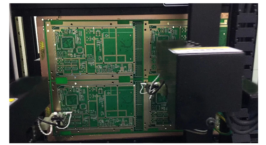
- A spectrum filter PCB should be reviewed as an RF network whose layout, material, and measurement path directly affect passband and stopband behavior.
- The first checks are filter topology, frequency range, substrate choice, launch design, grounding, shielding, and the test method used to validate insertion and return loss.
- Most filter-board failures show up as shifted center frequency, extra insertion loss, weak rejection, poor repeatability, or disagreement between simulation and measurement.
- Material choice matters, but copper geometry, coupling structures, via fences, connector launches, and enclosure interaction often decide whether the filter behaves as expected.
- Prototype success depends on freezing the measurement setup early, especially if the board will be validated with a VNA, tuned hardware, or spectrum-analyzer-based checks.
A spectrum filter PCB is a printed circuit board that implements or supports a frequency-selective RF filter, such as a bandpass, low-pass, high-pass, or notch structure. It needs careful control of dielectric behavior, conductor geometry, grounding, shielding, and RF measurement setup because small layout or fabrication shifts can change insertion loss, rejection, and center-frequency alignment.
Contents
- What to review first on a spectrum filter PCB
- Key design and validation rule table
- Early engineering trade-off table
- How substrate, coupling geometry, and grounding affect filter performance
- How RF measurement and tuning should be planned
- What prototype teams should lock down before release
- FAQ
- Next steps
- References
- Author and review
What to review first on a spectrum filter PCB
A spectrum filter PCB is not just a generic high-speed board with a filter circuit placed on it. The PCB itself is often part of the filter behavior. Line width, spacing, dielectric variation, launch design, enclosure coupling, and even measurement fixturing can move the final response.The first review points are usually:
- what filter type and frequency range the board is meant to realize or support
- whether the design is lumped, distributed, cavity-coupled, or a mixed topology
- which substrate family and copper profile match the loss, phase, and manufacturability needs
- whether the launch, connector, and ground strategy preserve the intended response
- how the board will be measured, calibrated, and compared against simulation after fabrication
For RF and microwave paths, it is usually worth comparing the structure against high-frequency PCB and Rogers PCB options before layout freeze.
Key design and validation rule table
| Rule / parameter | What to check first | Why it matters | How to verify | If ignored | | --- | --- | --- | --- | --- | | Filter topology fit | Match topology to bandwidth, rejection, and manufacturability target | The board structure depends on the actual filter behavior required | Schematic and EM review | Layout effort goes to the wrong architecture | | Substrate selection | Use material data that supports the intended frequency and tolerance needs | Dielectric behavior directly shifts filter response | Stackup review and laminate data review | Center frequency drift and inconsistent passband | | Coupling geometry | Control trace width, spacing, resonator geometry, and reference ground | Small geometry changes can move coupling and response shape | Layout inspection and simulation review | Poor rejection, ripple, or shifted response | | Launch and transition quality | Treat connectors, vias, and launches as part of the filter path | A weak launch can dominate the measured result | Launch review, [Gerber viewer](/tools/gerber-viewer/) inspection | Measurement looks worse than the actual filter core | | Shielding and grounding | Review via fences, enclosure interaction, and return continuity | Leakage paths and weak grounding reduce out-of-band control | Layout review and prototype check | Radiation, parasitic modes, unstable rejection | | VNA validation path | Freeze calibration and measurement setup early | Filter measurements are only credible when setup is repeatable | Test-fixture plan, calibration method, connector plan | Simulation-to-measurement mismatch with no clear cause |Early engineering trade-off table
| Design choice | Usually stronger for | Main trade-off | What to confirm early | | --- | --- | --- | --- | | Lumped filter implementation | Lower-frequency and compact designs | Component tolerance can dominate behavior | Tolerance stack and power handling | | Distributed microstrip / stripline filter | Higher-frequency planar RF implementations | More dependent on substrate and fabrication control | Material choice, copper profile, layout tolerance | | Lower-loss RF laminate | Better insertion-loss and stability margin | Higher cost and more process sensitivity | Frequency target, production route, availability | | More shielding and via fencing | Better isolation and cleaner stopband behavior | More layout area and possible tuning interaction | Enclosure fit, coupling sensitivity, rework access |How substrate, coupling geometry, and grounding affect filter performance
Filter PCBs do not respond only to ideal schematic values. Their real behavior comes from the interaction between substrate, geometry, and the way fields close through the board and enclosure.Three engineering questions usually matter most.
1. Is the substrate stable enough for the response target?
If the dielectric behavior moves too much with frequency or process variation, the realized filter can shift away from the simulated result. That does not always mean the board needs the most expensive material, but it does mean the substrate has to match the response target honestly.
2. Is the coupling geometry practical to fabricate?
The closer the filter behavior depends on narrow spacing or tight resonator geometry, the more fabrication tolerance matters. A design that only works in simulation but not in normal board tolerance is not ready for release.
3. Does the ground and shield structure support the intended RF path?
Weak via fences, incomplete return continuity, or enclosure interaction can create parasitic paths that flatten rejection or distort the passband. A quick Gerber viewer review often catches these issues before fabrication.
How RF measurement and tuning should be planned
A filter PCB is only useful when the measured result can be trusted. That means the measurement path has to be treated as part of the project, not as a last-minute lab detail.The most common review points are:
- whether the board will be validated primarily with a VNA, spectrum-analyzer workflow, or a tuned bench setup
- whether launches, calibration standards, and fixture assumptions are frozen before prototype release
- whether measured S-parameters, passband ripple, insertion loss, and rejection targets are defined in a way the board can actually prove
- whether any tuning or enclosure interaction is expected after first measurement
If the project is still early, PCB prototype, quick-turn PCB, and high-frequency PCB planning usually save more time than debating materials without a measurement plan.
What prototype teams should lock down before release
The most useful prototype is the one that proves the RF decision clearly. Before release, the filter team should decide what the first article is supposed to confirm and how it will be measured.A practical release checklist usually includes:
- Response target frozen
Define passband, stopband, insertion-loss, and return-loss expectations clearly enough to compare design and measurement. - Material and stackup identified
Use the intended substrate family and copper assumptions in the release package. - Launch and fixture path approved
Confirm connectors, transitions, and calibration method before ordering the board. - Measurement method defined
Decide whether validation will rely on VNA S-parameters, spectrum-domain checks, or both. - Revision and assembly data aligned
Keep BOM, tuning notes, stackup, and build revision synchronized. A BOM viewer review helps prevent unexpected component substitutions on mixed lumped/distributed designs.
FAQ
What is the first thing to check on a spectrum filter PCB?
Start with filter topology, substrate choice, and the measurement method that will prove the result. Those three decisions usually determine whether the rest of the design work is aligned.
Is substrate choice the only thing that controls filter performance?
No. Geometry, connector launch, ground continuity, shielding, and fabrication tolerance can all move the final response.
Why do filter PCBs often disagree with simulation?
Because simulation assumptions about dielectric behavior, copper, transitions, or measurement setup may not match the actual fabricated and measured structure closely enough.
When should a team use a VNA to validate a filter PCB?
A VNA is usually the strongest choice when the board must prove S-parameter behavior such as insertion loss, return loss, passband shape, and rejection across frequency.
What should be frozen before the first prototype release?
Freeze the filter response target, substrate family, launch strategy, calibration method, and the exact measurement workflow for the first article.
Next steps
If you are developing a spectrum filter PCB, the most useful next step is usually to review substrate, coupling geometry, launch design, and validation setup as one RF system.HILPCB can support that process through:
- High-frequency PCB planning for RF and microwave filter structures
- Rogers PCB review when dielectric stability and lower loss matter
- PCB prototype and quick-turn PCB support for early measurement builds
- Gerber viewer checks during launch and grounding review
- Request a quote when your stackup, BOM, and validation plan are ready for review