
[English translation result]
- Volume: Excessive solder paste can cause bridging shorts; insufficient amounts may lead to weak soldering or open circuits.
- Area: Inadequate coverage area can affect soldering strength.
- Height: Uneven solder paste height may cause chip tilting during reflow soldering (the "tombstoning" effect).
- Offset: Misalignment of solder paste from the pad center may result in soldering deviations and bridging.
For complex HBM3 interposer PCB layouts, the dense I/O arrays pose significant challenges to SPI's detection accuracy and speed. Once SPI detects a printing defect, the system immediately triggers an alarm, allowing operators to promptly clean the stencil and adjust printing parameters. This prevents defective boards from entering costly reflow soldering and chip mounting processes, significantly improving the First Pass Yield (FPY) and laying a solid foundation for subsequent assembly quality.
Comparison of SPI, AOI, and X-Ray Inspection Technologies
| Inspection Technology | SPI (Solder Paste Inspection) | AOI (Automated Optical Inspection) | X-Ray (X-Ray Inspection) |
|---|---|---|---|
| Inspection Target | Solder paste on pads | PCB/substrate surface features, components | Internal structures, solder joints, vias | Core Capabilities | 3D profile measurement (volume, height, area) | 2D/3D image comparison, color recognition | Non-destructive X-ray imaging |
| Main Defects Detected | Excessive/insufficient solder paste, bridging, misalignment, solder spikes | Open/short circuits, missing/misaligned components, reversed polarity | BGA voids, cold solder joints, inner layer alignment, microvia filling |
| Application Stage | After solder paste printing, before component placement | After etching, after solder mask, after reflow soldering | After reflow soldering, during reliability testing |
What is the Critical Role of AOI in Fine Line and RDL Layer Manufacturing?
When IC substrates enter the circuit manufacturing stage, AOI begins to play its pivotal role. In AI chip substrates, the RDL layer carries high-speed signals from the chip I/O to the ball grid array (BGA) package. The width and spacing of these circuits may be as small as 10μm/10μm or even less, where any minor defect can have fatal consequences for signal integrity.
Modern AOI systems employ multi-source lighting (e.g., ring light, coaxial light) and high-resolution line scan cameras to capture fine details on the substrate surface. By performing pixel-level comparisons with Gerber design files, AOI can quickly identify the following defects:
- Open and short circuits: The most common fatal defects directly causing functional failure.
- Line width/spacing violations: Affecting characteristic impedance, leading to signal reflection and crosstalk.
- Residual copper and mouse bites: Potential reliability risks that may fracture under thermal stress.
- Pad defects: Contaminated or damaged pads may affect subsequent soldering quality.
- Solder mask alignment: Narrow or misaligned solder mask bridges may cause short circuits during soldering. For HDI (High-Density Interconnect) boards, AOI is equally crucial in microvia HDI stack validation. It inspects the cleanliness, shape, and positional accuracy of laser-drilled hole openings after each layer, ensuring the quality of subsequent electroplating and via filling. By performing AOI after each critical process step, manufacturers can establish robust process control capabilities, guaranteeing flawless layer stacking. Professional HDI PCB manufacturers like HILPCB leverage advanced AOI equipment to ensure the exceptional quality of their high-density products.
How Does X-Ray Inspection Reveal Internal Risks in Microvia Stacking?
If AOI is like examining the skin, then X-Ray is akin to performing a CT scan. For increasingly complex AI chip substrates, many critical defects lie beneath the surface and can only be detected by X-Ray. Especially in microvia HDI stack validation, X-Ray inspection is irreplaceable.
Microvias are key to achieving vertical interconnections between layers in HDI boards, with diameters typically smaller than 75 microns. In multilayer stacked microvia structures, any poorly filled via can become a "time bomb." X-Ray inspection enables:
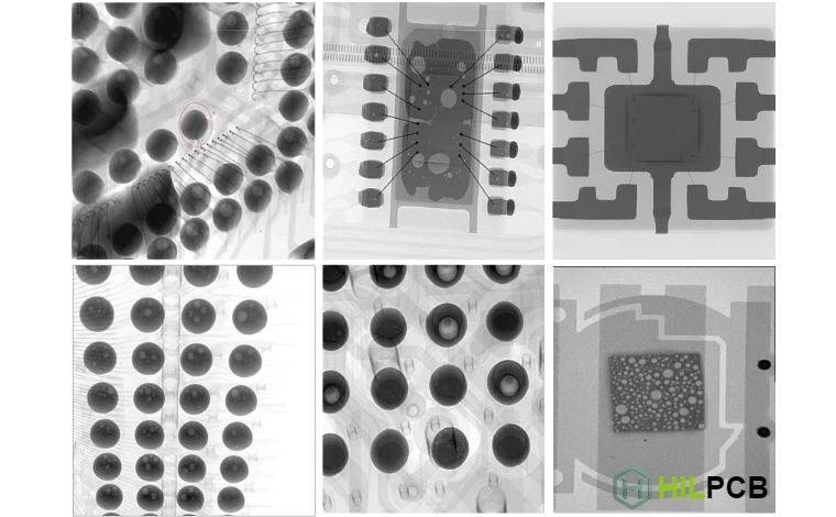
- Microvia filling inspection: By analyzing differences in X-ray absorption rates, it clearly reveals whether electroplated copper fully fills the blind vias and whether voids exist. Voids severely impact current conduction and heat dissipation, leading to cracking due to stress concentration during thermal cycling.
- Layer-to-layer alignment accuracy assessment: X-Ray can simultaneously image multiple circuit layers, precisely measuring the alignment between inner and outer layers, as well as patterns across layers. Misalignment can cause drilling deviations from pads, resulting in connection failures.
- BGA/μ-bump solder joint quality inspection: After chip assembly, X-Ray is the gold standard for inspecting BGA and micro-bump solder joints. It detects internal voids, head-in-pillow effects, cracks, and bridging defects—flaws invisible to optical methods.
Additionally, selecting the right microvia HDI stack materials is critical for both inspection and reliability. Advanced dielectric materials like low-CTE (Coefficient of Thermal Expansion) core boards and ABF (Ajinomoto Build-up Film) reduce thermal stress, but their material properties also require X-Ray system optimization for optimal imaging contrast.
Key Inspection Checklist for EMIB Interconnect Boards
This is a simplified EMIB interconnect board checklist, covering critical inspection points from design to manufacturing.
- Design Phase (DFM): Verify the dimensional tolerances of EMIB embedded cavities and the microbump pad layout to ensure they meet manufacturing capabilities.
- Substrate Fabrication (AOI): Perform 100% AOI on high-density circuits connected to EMIB to ensure no open/short circuits, with line width accuracy controlled within ±5%.
- Cavity Formation (3D Scanning): Use 3D optical profilometers or X-Ray scanning to validate cavity depth and bottom flatness, ensuring smooth EMIB chip embedding.
- Post-Chip Assembly (X-Ray): Conduct 3D AXI inspection on microbumps between EMIB and the substrate to check void rates, bridging, and alignment.
- Final Testing (Functional + Reliability): Perform signal integrity tests (TDR/VNA) and accelerated aging tests (e.g., thermal cycling) to validate long-term interconnect reliability.
How to Integrate SPI/AOI/X-Ray for Comprehensive Manufacturing Process Control?
Using SPI/AOI/X-Ray inspection technologies in isolation offers limited value. Their true power lies in integrating them into a closed-loop, data-driven Statistical Process Control (SPC) system. This embodies the Industry 4.0 philosophy in PCB/IC substrate manufacturing.
An integrated inspection system enables:
- Feed-forward: For example, slight alignment offset data detected by AOI in inner layers can be passed to subsequent drilling processes to automatically fine-tune drilling coordinates for compensation.
- Feedback: If SPI consistently detects insufficient solder paste volume, the system can automatically alert the upstream solder paste printer to adjust stencil squeegee pressure or clean the stencil. Similarly, if X-Ray detects rising BGA void rates, the data can feedback to the reflow soldering process to optimize the temperature profile.
- Data Traceability and Analysis: Assign a unique ID to each board and record all inspection data at every node. When final product failures occur, the specific manufacturing batch, equipment, and parameters can be quickly traced for root cause analysis. This intelligent process control transforms the traditional "inspect afterward, reject defective products" model into an advanced "real-time monitoring, defect prevention" approach. As a technology-driven manufacturer, HILPCB is committed to continuously optimizing its manufacturing processes through this data-driven method, delivering highly consistent and reliable products to customers. This relentless pursuit of quality is critical for AI and data center applications that demand zero defects.
What Are the Special Inspection Considerations for HBM3 Interposer PCB Layouts?
HBM3 (3rd Generation High Bandwidth Memory) and its subsequent versions are standard for AI accelerators, connecting to processor cores via thousands of parallel data lines on silicon interposers. The design and manufacturing of HBM3 interposer PCB layouts represent one of the most challenging aspects of the entire packaging technology chain.
Special inspection considerations include:
- Ultra-High Resolution AOI: The line width and spacing for HBM interconnects typically operate at the 2μm/2μm level, far exceeding traditional PCBs. This demands AOI systems with sub-micron optical resolution and exceptionally precise detection algorithms.
- Warpage Compensation: Both silicon and organic interposers can experience warpage during manufacturing and assembly. Inspection systems (particularly AOI and SPI) must incorporate real-time 3D height measurement and compensation capabilities to ensure accurate focusing and measurements on warped surfaces.
- TSV and Microbump Connection Verification: HBM stacks achieve vertical interconnects through Through-Silicon Vias (TSVs). X-Ray inspection must not only examine microbumps between the interposer and HBM base but also assess TSV integrity and their connections to solder joints, requiring higher-energy and higher-resolution X-Ray equipment.
- Impedance Uniformity: For these high-speed parallel buses, impedance control is critical. While AOI primarily checks geometric dimensions, its measurement data can be fed into simulation tools to indirectly evaluate impedance consistency. Some advanced high-speed PCB manufacturers also integrate TDR (Time Domain Reflectometry) testing for 100% electrical performance validation of critical lines.
HILPCB Advanced Substrate Manufacturing & Inspection Service Value
| Service Feature | Customer Benefit |
|---|---|
| Comprehensive SPI/AOI/X-Ray Inspection Capabilities | End-to-end quality assurance from source to finished product, ensuring product reliability. |
| Expertise in IC Substrates and HDI Technology | Capable of handling the most complex micro-blind via stacking and fine-line designs to achieve higher performance. |
| Free DFM/DFA Analysis | Optimize designs before production to enhance manufacturability, reduce costs, and mitigate risks. |
| One-Stop Manufacturing and Assembly Services | Simplify supply chain management, shorten time-to-market, and ensure seamless integration across all stages. |
What Stricter Requirements Do Automotive-Grade Applications Impose on Inspection Standards?
As AI technology penetrates safety-critical fields like autonomous driving, the demand for automotive-grade HBM3 interposer PCBs has emerged. Automotive electronics impose far more stringent reliability requirements than consumer electronics, necessitating compliance with rigorous standards such as AEC-Q100 (for chips) and AEC-Q200 (for passive components).
This places higher demands on SPI/AOI/X-Ray inspection:
- Zero-Defect Target: The automotive industry pursues failure rates at the PPB (parts per billion) level. This means inspection systems must be capable of detecting all minor anomalies that could lead to long-term failures, not just functional defects.
- Stricter Acceptance Criteria: For example, while consumer-grade products might accept BGA solder joint void rates below 25%, automotive-grade applications may require rates below 10%, with even lower thresholds for critical solder joints.
- 100% Full Inspection and Traceability: Every automotive-grade substrate shipped must undergo 100% AOI and X-Ray inspection, with all images and data archived to ensure full traceability. In the event of a recall, problematic batches can be precisely identified.
- Accelerated Aging Tests Combined with Inspection: Products must endure harsh temperature cycling (-40°C to 125°C), vibration, and humidity tests. Non-destructive inspection methods like X-Ray are used before and after these tests to evaluate microstructural changes and ensure reliability throughout the product lifecycle.
Meeting these requirements demands not only top-tier inspection equipment but also a mature quality management system compliant with IATF 16949 standards. This covers every detail, from the selection of microvia HDI stack materials to final testing.
Why Is Choosing a PCB Manufacturer with Advanced Inspection Capabilities Critical?
In the high-risk, high-value field of AI chip interconnects and carrier board PCBs, the decision to choose a manufacturing partner is critical. A seemingly minor cost-saving measure, if achieved at the expense of inspection processes, may ultimately result in millions of dollars in losses and project delays. Therefore, evaluating a manufacturer's SPI/AOI/X-Ray inspection capabilities is a core aspect of assessing their overall technical strength.
A partner with advanced inspection capabilities, such as Highleap PCB Factory (HILPCB), can provide you with:
- Higher product yield: Maximizes final product qualification rates by identifying and correcting issues early in the manufacturing process.
- Greater design flexibility: Robust manufacturing and inspection capabilities enable support for more aggressive, compact designs, helping you achieve your product performance goals.
- Faster time-to-market: Reliable manufacturing processes reduce rework and debugging time, accelerating the journey from prototype to mass production.
- Lower total cost of ownership: High-quality carrier boards and interconnects ensure long-term reliability of end products, reducing field failure rates and warranty costs.
HILPCB has deep expertise in the field of IC Substrate PCB. Their production lines are equipped with industry-leading inspection equipment and staffed by an experienced engineering team that thoroughly understands the unique requirements of AI chips for carrier boards. From DFM (Design for Manufacturability) reviews during the design phase to comprehensive process control through inspection methods, and offering turnkey assembly services from carrier board manufacturing to chip packaging, HILPCB is committed to being your reliable partner on the path to AI hardware innovation.
Conclusion: Inspection Technology is the "Eyes" Illuminating AI's Future
In summary, SPI/AOI/X-Ray inspection technologies have evolved from traditional quality control tools into core enabling technologies driving the advancement of advanced packaging. In the precision world of AI chips, composed of tens of thousands of microscopic connections, these three technologies serve as tireless "eyes," safeguarding the integrity of every signal pathway, solder joint, and internal structure. They are crucial for ensuring successful microvia HDI stack validation, optimizing HBM3 interposer PCB layout manufacturing, and meeting the stringent standards of automotive-grade HBM3 interposer PCB.
As AI chips continue to evolve toward higher performance and greater integration, the demands on inspection technologies will also keep rising. Future inspections will become more intelligent, data-driven, and deeply integrated with AI algorithms to achieve predictive maintenance and adaptive process control. Choosing a manufacturer like HILPCB—one that not only possesses advanced manufacturing processes but also deeply understands and heavily invests in core inspection capabilities such as SPI/AOI/X-Ray inspection—will be a critical step toward success in the competitive AI market.
Common Questions
Why are SPI, AOI, and X-ray all needed for AI chip interconnect products?
Fine-pitch AI assemblies can fail in solder paste, visible joints, and hidden internal structures, so one inspection method is not enough.
What hidden issues does X-ray help detect?
It is especially useful for voids, opens, shorts, head-in-pillow risk, and hidden solder problems under advanced packages or interconnect structures.
How do these inspections support advanced packaging?
They help validate microvia HDI stacks, fine redistribution layers, interposer assemblies, and other dense AI interconnect features.
Why is closed-loop SPC valuable here?
Inspection data can trigger early process adjustments, reducing drift and improving yield as package complexity increases.