
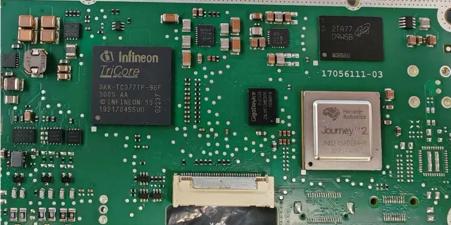
With the rapid electrification and intelligence wave in automotive electronics, ADAS and EV power systems are evolving faster than ever. At the center of these systems are PCBs that carry both complex computing and high-power transfer. Unlike consumer electronics, automotive PCBs must survive vibration, extreme temperature, and high-voltage/high-current stress—where even a tiny manufacturing defect can lead to catastrophic consequences. That’s why a comprehensive, precise quality-control system is essential, and SPI/AOI/X-Ray inspection is a core pillar that enables automotive-grade reliability and high-voltage safety.
From early DFM/DFT/DFA review, to precision soldering in production, to final functional verification, every step must pursue near-zero defects. For high-voltage assemblies such as BMS, OBC, and inverters, the combination of power devices, heavy copper routing, and dense interconnect pushes process stability and inspection “penetration” to the limit. In this article, from a BMS design expert’s perspective, we explain how SPI/AOI/X-Ray inspection works together with Traceability/MES, advanced processes like Selective wave soldering, and a disciplined test strategy to build both the first and last safety line for automotive electronics.
SPI/AOI/X-Ray inspection: the foundation of zero-defect automotive manufacturing
In modern PCBA production lines, SPI/AOI/X-Ray inspection forms a “three-in-one” automated inspection loop. Each tool serves a different stage, together protecting quality from solder paste printing to placement and final solder formation.
SPI (Solder Paste Inspection) — the defect-prevention “whistleblower” SPI sits after the printer and before placement as the first quality gate. More than 70% of SMT solder defects originate from poor printing. Using laser or structured-light scanning, SPI measures paste in 3D and quantifies volume, area, height, offset, and shape per pad. On automotive power PCBs, power MOSFET/IGBT thermal pads are extremely sensitive to paste volume. Too much paste can cause floating or solder balls during reflow, leading to shorts; too little causes insufficient joints and poor thermal conduction, creating hotspots that reduce lifetime and safety margin. SPI catches these deviations early so engineers can intervene before defects form.
AOI (Automated Optical Inspection) — the “patrol” for process monitoring AOI typically follows reflow and uses high-resolution cameras and image algorithms to inspect the PCBA quickly and comprehensively. It detects wrong/missing parts, polarity errors, offset, tombstoning, and visible solder issues like bridging, insufficient/excess solder, and cold joints. On ADAS boards with extremely high component density (thousands of 0201 or even 01005 parts), manual inspection is not realistic. AOI’s speed and consistency protect large-scale production quality. However, AOI is surface-limited and cannot see hidden joints under BGA/LGA/QFN or areas shadowed by large heatsinks.
X-Ray Inspection (AXI) — the “X-ray vision” for deep diagnostics AXI closes AOI’s blind spots and is indispensable for high-reliability automotive electronics. X-Ray penetrates structures to produce 2D/3D images of internal joints:
- BGA/QFN joint analysis: for ADAS processors and sensor ICs in BGA packages, AXI checks ball shape/size/alignment and detects bridging or Head-in-Pillow.
- Voiding on power-device thermal pads: on EV power boards, thermal pad solder quality directly affects thermal management. X-Ray quantifies Voiding; IPC commonly requires voiding below 25%. Excess voiding blocks heat flow and is a major cause of overheating failures.
- Through-hole fill verification: for high-current connectors or Press-fit pins using THT/through-hole soldering, X-Ray verifies Hole-fill to ensure long-term electrical and mechanical reliability.
Together, these three methods create a full quality chain—from surface to internal, from prevention to final diagnosis—and are essential enablers for automotive functional safety targets (ISO 26262).
DFM/DFT/DFA review: eliminating high-voltage and high-current risk at the source
End-of-line inspection alone is not enough—real quality starts in design. A complete DFM/DFT/DFA review is the key to manufacturability, testability, and assembly readiness. At HILPCB, we treat it as a foundation for project success.
DFM (Design for Manufacturability): we focus on high-voltage creepage/clearance compliance (e.g., IEC 60664-1). For high-current paths, we review copper thickness and trace width and often recommend heavy copper PCB. We also optimize pad design, solder mask openings, and silkscreen clarity to match SPI/AOI/X-Ray inspection capabilities—reducing false calls caused by design issues.
DFT (Design for Testability): DFT ensures the product can be tested efficiently and thoroughly, including reserving sufficient test pads for ICT and FCT. A rational test-point layout is the basis of Fixture design (ICT/FCT)—reducing fixture complexity/cost and improving coverage.
DFA (Design for Assembly): we review placement to avoid shadowing effects from tall parts over small parts during soldering—especially with Selective wave soldering. We also evaluate orientation and spacing for automated placement to reduce assembly risk. A strong DFM/DFT/DFA review can eliminate over 90% of potential manufacturing/test issues before design freeze.
Key reminder: design is the first line of defense
- High-voltage safety: enforcing creepage/clearance rules in DFM is the first measure to prevent HV breakdown.
- Test coverage: solid DFT decisions directly determine ICT/FCT effectiveness and the baseline for functional validation.
- Assembly yield: good DFA placement reduces soldering shadow effects and improves first-pass yield for mixed technology (SMT+THT).
- Inspection efficiency: designing for SPI/AOI/X-Ray inspection (e.g., fiducials) improves inspection accuracy and throughput.
EV power-board thermal structures: coordinated heatsinks, VC, and cold plates
EV power density keeps rising, making thermal management a primary design constraint. The PCB is not only an electrical carrier, but also a critical thermal conduction path.
TIM and PCB thermal design: heat from power devices must transfer through the PCB to a Heat Spreader, Vapor Chamber (VC), or Cold Plate. The bottleneck is often the interface. We use large copper pours and dense Thermal Vias to move heat quickly from the device to the PCB backside. For extreme thermal needs, MCPCB is an ideal option because the metal core itself acts as a strong heat spreader.
Solder quality and thermal resistance: the solder layer between the device thermal pad and the PCB is one of the most critical points in the heat path. Any solder defect—especially Voiding—creates insulating air pockets that sharply increase thermal resistance and drive local temperature rise. This is where SPI/AOI/X-Ray inspection is decisive: SPI ensures accurate paste volume to support low-void joints, and X-Ray is the final “judge” that quantifies voiding to keep every critical thermal path open—protecting long-term reliability at full load.
Busbar and heavy copper: reliable design and inspection for high-current paths
In applications such as BMS and inverters, currents can reach hundreds of amps. Standard PCB traces cannot carry this reliably; special solutions are required.
Heavy copper and busbar integration: heavy copper PCBs (copper thickness ≥ 3oz) are the base for high-current paths. With controlled etching, we can build wide traces that carry current stably. When current goes higher, preformed Busbar structures are integrated via soldering or Press-fit. This improves current capacity and also increases mechanical strength.
Connection challenges and inspection:
- THT/through-hole soldering: for busbar pins or high-current connectors, full Hole-fill (100%) is required to minimize contact resistance and maximize mechanical reliability. This often uses Selective wave soldering or hand soldering, supported by strict AOI and X-Ray checks.
- Press-fit: a solderless connection that presses a specially shaped pin into a plated hole to form a gas-tight “cold weld.” It avoids soldering thermal shock and can be highly reliable. But verification is challenging and often requires X-Ray to inspect hole-wall deformation and pin seating.
HILPCB capability: handling extreme electrical challenges
- ✓Heavy copper manufacturing: supports heavy copper PCBs up to 12oz for high-current applications.
- ✓Busbar integration: extensive busbar/PCB integration experience, supporting soldering, Press-fit, and other reliable connection options.
- ✓Precision inspection: advanced 3D SPI, high-resolution AOI, and 3D X-Ray to ensure every high-current joint meets quality targets.
- ✓Automotive standards: strict IATF 16949 quality system compliance for automotive-grade manufacturing.
Fixture design (ICT/FCT) and Traceability/MES: end-to-end traceability and functional validation
Inspection doesn’t stop at manufacturing—electrical performance validation is equally important.
Precision Fixture design (ICT/FCT):
- ICT (In-Circuit Test): probes contact predefined test points to measure component values (R/C, etc.) and detect opens/shorts. For high-voltage boards, Fixture design (ICT/FCT) must account for probe clearance and voltage rating.
- FCT (Functional Test): simulates real operating conditions, applies input signals, and verifies outputs against spec. For BMS, FCT may emulate cell voltages and temperature signals and verify balancing/protection functions. A strong Fixture design (ICT/FCT) ensures efficient, reliable testing.
Traceability/MES: In automotive manufacturing, traceability is mandatory. Traceability/MES assigns a unique QR identity to each PCBA and binds material lots, SPI data, placement feeder IDs, reflow profiles, AOI/X-Ray results, and ICT/FCT data to that ID. If issues occur later, Traceability/MES enables instant end-to-end history retrieval, rapid root-cause location, and accurate containment of affected lots—critical for recall control and continuous improvement. Choosing a partner like HILPCB with integrated turnkey assembly services provides this traceability by default.
Mixed-technology soldering: Selective wave soldering and THT reliability
Even though SMT dominates, THT/through-hole soldering remains critical in automotive electronics due to mechanical strength and current capacity—especially for power connectors and large inductors/capacitors.
When adding THT parts after SMT placement and reflow, traditional wave soldering can damage SMT components. Selective wave soldering becomes the best option: a micro nozzle solders only the required THT pin areas with molten solder, avoiding the rest of the board.
Selective wave soldering requires tighter process control: preheat temperature, dwell time, and nozzle speed must be tuned to achieve good Hole-fill and joint shape. After soldering, AOI checks surface shape/gloss and solder balls, and X-Ray confirms internal Hole-fill to avoid latent reliability risks. For complex through-hole assembly, disciplined control plus multi-layer inspection is the key.
Assembly strengths: mixed-technology expertise
- Advanced equipment: multiple selective wave soldering systems to handle different board types and layouts.
- Process experts: experienced engineers tune optimal parameters per product to secure solder quality.
- Comprehensive inspection: AOI + X-Ray for 100% inside/outside checks of THT joints.
- System integration: seamless integration of THT process data into Traceability/MES for end-to-end traceability from SMT to THT.
Conclusion
Automotive ADAS and EV power PCBs push PCBA manufacturing to a new level of reliability and safety. A single inspection tool or process is not enough. A comprehensive quality system centered on SPI/AOI/X-Ray inspection, spanning design, manufacturing, and test, is the only proven path to success.
From early risk elimination via DFM/DFT/DFA review, to tight process monitoring with SPI/AOI/X-Ray inspection, to mixed-technology execution with Selective wave soldering, and finally to functional validation and traceability via Fixture design (ICT/FCT) and Traceability/MES—each link matters. As a trusted partner, HILPCB combines advanced equipment, deep automotive process understanding, and a strict quality culture to deliver automotive-grade PCBs and assembly services that meet the toughest standards—helping you move forward with confidence in the future of automotive electronics.
Common Questions
Why is inspection stricter for ADAS and EV electronics?
These products combine safety-critical functions, automotive reliability expectations, and, in many cases, high-voltage power conditions.
How do SPI, AOI, and X-ray fit with DFM, DFT, and DFA?
Design review removes risk before build, while inspection verifies real process output and catches defects throughout manufacturing.
What other processes are usually part of the quality chain?
Selective wave soldering, THT control, ICT or FCT fixtures, and full MES traceability are common for mixed-technology automotive boards.
What is the goal of this inspection strategy?
The objective is near-zero-defect production with documented quality control from prototype through mass production.