
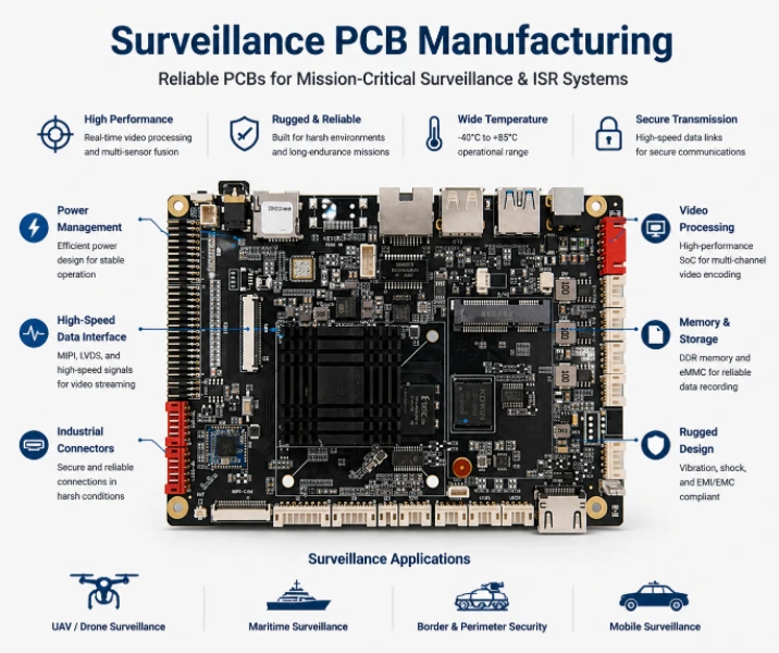
The global military ISR market is valued at $32.4 billion and growing at 5.8% CAGR through 2030, driven by UAV proliferation and multi-sensor payload integration. Surveillance systems—mounted on unmanned aerial vehicles, fixed installations, naval vessels, or ground vehicles—share a common electronic backbone: sensors capture imagery and signals, processing boards extract actionable intelligence, data links transmit to operators, and all of this runs continuously for hours or days on constrained power budgets. The PCBs within these systems define the platform's surveillance capability: sensor resolution, processing throughput, data link bandwidth, and operational endurance.
ISR platforms operated by the United States, United Kingdom, France, Germany, Canada, and Australia—from the MQ-9 Reaper to the Watchkeeper and Heron—generate terabytes of intelligence data per mission. The PCBs processing this data must meet both real-time performance demands and environmental survival across operating theaters from the Middle East to the North Atlantic maritime patrol zone.
Modern ISR payloads integrate multiple modalities—electro-optical (EO), infrared (IR), synthetic aperture radar (SAR), and signals intelligence (SIGINT)—fusing their outputs into a unified picture. Each modality has distinct PCB requirements, and the fusion processor combining them demands the high-speed, high-density board design typical of advanced computing platforms.
HILPCB Manufacturing Capability: We fabricate surveillance system PCBs with HDI via structures for dense FPGA processing boards, low-loss RF laminates for data link modules, heavy copper thermal management for continuous operation, and IPC-6012 Class 3 qualification for defense ISR programs.
In This Guide
- Sensor Interface Boards for EO, IR, and SAR Payloads
- Video Processing and Multi-Sensor Fusion PCB Design
- Data Link and Encrypted Communication Boards
- Power Management and SWaP Optimization
- Ruggedization and Environmental Qualification
- HILPCB Surveillance PCB Manufacturing
Sensor Interface Boards for EO, IR, and SAR Payloads
Surveillance sensor interface boards condition raw sensor outputs for digitization — handling CCD/CMOS video signals, infrared detector readouts, or radar IF signals. Each sensor modality places distinct demands on the PCB that must be addressed through coordinated material selection, layout isolation, and power architecture.At HILPCB, our sensor interface board designs address the mixed-signal isolation challenges of multi-sensor ISR payloads — ensuring that cryocooler compressor drive, high-speed video clocks, and precision analog measurement coexist without mutual degradation.
Multi-Sensor Interface Design
- EO Camera Interface: Large-format CMOS sensors (20–100 MP, 30–120 fps) requiring stable bias with <500 μV ripple, pixel clock distribution at 50–200 MHz with <100 ps jitter, and LVDS/SLVS-EC data output at 1–4 Gbps per lane on high-speed controlled-impedance layers.
- Infrared Sensor Interface: Cooled MWIR/LWIR detectors with cryocooler drive circuits (30–60 Hz switching at 10–30 W) isolated from detector readout electronics — achieving the >80 dB isolation that detector-limited NETD performance demands.
- SAR Radar Interface: X-band (9.5 GHz) or Ku-band (16 GHz) signal conditioning requiring low-loss RF material, wideband receive with 500 MHz–2 GHz bandwidth, and 12–14 bit ADCs at 2–4 GSPS.
- Lens Control: Motor drivers for zoom/focus/aperture integrated on the sensor board with isolated power and ground routing preventing motor noise from contaminating sensor readout.
Validated Sensor Performance
Every sensor interface board undergoes noise floor verification using reference signal injection, confirming that the PCB contribution stays below the sensor noise floor — preserving the image quality that intelligence analysts depend on for target identification. Fixed-site commercial systems built on smart surveillance camera PCBs face lighter environmental limits, but the same noise-floor discipline applies.
Video Processing and Multi-Sensor Fusion PCB Design
The processing board is the computational engine of any surveillance system. Modern ISR platforms use FPGAs (Xilinx Zynq UltraScale+, Intel Stratix 10) or embedded GPUs for real-time image enhancement, target detection, tracking, and sensor fusion — generating the intelligence products that drive mission decisions.At HILPCB, our ISR processing board fabrication delivers the layer count, signal integrity, and thermal management that 14–20 layer FPGA-centric designs demand — from multilayer stack-up design through production assembly.
Processing Board Architecture
- FPGA/GPU Platform: 14–20 layer boards carrying 1500+ pin BGA packages at 0.8–1.0 mm pitch with HDI escape routing, multiple DDR4/DDR5 memory banks, PCIe Gen 4 and 10/25GbE serial interfaces, and 30–80 W processor power delivery.
- Sensor Fusion: Pixel-level or decision-level fusion combining time-stamped EO, IR, and radar data — requiring GPS-disciplined clock distribution via matched-length LVPECL traces for precise inter-sensor synchronization.
- Data Recording: NVMe/PCIe storage interfaces for terabyte-scale mission data capture, with write-endurance monitoring and AES-256 encryption for classified data at the storage controller level.
- SMT Assembly with J-STD-001 Class 3 soldering ensures the solder joint reliability that 6–24 hour continuous ISR missions demand.
Data Link and Encrypted Communication Boards
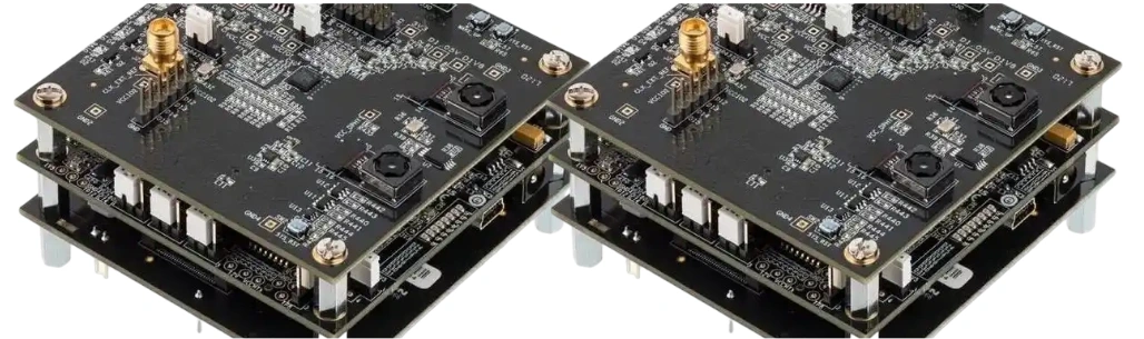
Surveillance data must reach ground control in real-time — often over 50–200 km from UAV platforms. The data link board combines digital modem processing, RF signal conditioning, and encryption into a single hybrid-material assembly that bridges the digital and RF domains.At HILPCB, our data link board fabrication combines low-loss RF materials for C/Ku/Ka-band signal layers with standard high-Tg FR-4 for digital sections — delivering the hybrid stack-ups that wideband military data links demand at production quality.
Data Link PCB Engineering
- RF Architecture: C-band (4–8 GHz), Ku-band (12–18 GHz), or Ka-band (26–40 GHz) sections on low-loss material with controlled impedance to ±5%. VNA verification to 20 GHz validates RF performance before shipment.
- Digital Modem: FPGA implementing waveform generation and demodulation on standard FR-4 layers within the same hybrid stack-up, with DAC/ADC interfaces bridging the digital and RF domains.
- COMSEC/Encryption: Type 1/2 encryption module with tamper-protected key storage, hardware AES engines, and TEMPEST compliance through additional shielding and filtered I/O.
- Antenna Integration: Impedance-controlled antenna feed transitions and matching networks optimized for the specific antenna architecture — panel, dish, or conformal.
Power Management and SWaP Optimization
ISR platforms — especially UAVs — prioritize power efficiency because every watt consumed by electronics reduces fuel capacity and mission duration. A surveillance payload drawing 200 W instead of 150 W can reduce UAV endurance by 30 minutes on a 6-hour mission.At HILPCB, our power and SWaP engineering for surveillance electronics targets both electrical efficiency and physical miniaturization — using heavy copper power delivery for low losses and HDI construction for maximum density.
Power and SWaP Optimization
- Efficient Conversion: GaN FET-based synchronous buck converters achieving >95% efficiency at 12V-to-1V conversion ratios typical of FPGA core supplies — versus 85% from linear regulators, saving 15 W per board.
- Multi-Mode Operation: Independent enable/disable for each sensor and processor section. When radar is not needed, its power section shuts down completely — not standby.
- HDI Miniaturization: Reducing board area 30–40% versus standard through-hole via designs through laser-drilled microvias, 0201/01005 passives, and embedded passives — directly reducing payload weight.
- Power Board Design: 28 VDC platform input converted to 12V, 5V, 3.3V, 1.8V, 1.2V, 0.85V rails with EMI filtering, current monitoring telemetry, and heavy copper planes for low I²R loss.
Ruggedization and Environmental Qualification
Surveillance electronics operate from desert airstrips to North Atlantic patrol aircraft to vibrating ground vehicles — environments spanning the full severity range of MIL-STD-810H. PCB construction must survive this reality across continuous mission durations and multi-year service lifetimes.At HILPCB, our ruggedization approach matches materials and processes to the specific platform environment — from high-altitude UAV payloads to salt-fog-exposed naval installations.
Platform-Specific Environmental Design
- UAV Payloads: -40°C to +71°C operation at altitudes to 25,000 ft. Reduced atmospheric pressure affects component voltage ratings and dielectric withstand — verified through altitude chamber testing.
- Naval Installations: Salt fog survival per MIL-STD-810H with ENIG surface finish and silicone conformal coating rated for continuous 95% RH exposure.
- Ground Vehicles: 5–500 Hz vibration at 4G with component underfill on critical BGAs, corner staking on large passives, and strain relief on all connectors.
- Fixed Sites: Continuous 24/7 operation for years requiring thermal design validated for steady-state maximum ambient, not just short-duration peaks.
Production Qualification
Each surveillance PCB undergoes 100% electrical test, impedance verification on RF layers, burn-in at +55°C for 72 hours (defense programs), and EMI/EMC pre-screening per MIL-STD-461G to verify co-located subsystem compatibility.
HILPCB ISR and Surveillance Electronics Programs
HILPCB serves ISR and surveillance electronics programs for defense contractors and government agencies across the United States, United Kingdom, Germany, France, Canada, and Australia. Our capabilities span the full range of surveillance PCB requirements:
- 14–20 layer processing boards with HDI FPGA escape, back-drilling for >5 Gbps signals, and heavy copper power delivery
- Hybrid Rogers/FR-4 data link boards with impedance control to ±5% and VNA verification
- Mixed-signal sensor interface boards with >80 dB isolation between high-power and precision analog sections
- Rigid-flex construction for SWaP-constrained payloads where connectors add unacceptable weight
- IPC-6012 Class 3 fabrication with full material traceability and export control compliance
- From prototype through production, with turnkey assembly delivering fully tested subsystem boards
Surveillance PCB FAQ
How do surveillance PCBs handle mixed-signal isolation for multiple sensors?
ISR payloads fuse data from EO, IR, and SAR sensors, combining sensitive analog detectors, high-speed digital processors, and high-power cryocoolers. Achieving >80 dB of isolation requires multi-layer stack-ups with dedicated stripline shielding, star-point grounding architectures, and physical separation of noisy motor drivers from low-noise analog inputs.
Why is SWaP (Size, Weight, and Power) optimization crucial for UAV PCBs?
Every watt of power and gram of weight consumed by the payload electronics directly reduces the UAV's fuel capacity and mission endurance. We optimize SWaP by using high-efficiency GaN power converters (saving watts) and High Density Interconnect (HDI) structures with microvias (reducing board size and weight by up to 40%).
How are surveillance PCBs ruggedized for high-altitude UAV operations?
High-altitude operations (-40°C, low pressure) stress components and alter dielectric withstand voltages. Boards are engineered with high-Tg materials, conformal coating to protect against condensation during rapid descents, and underfill on critical BGA components to survive continuous engine vibration.