
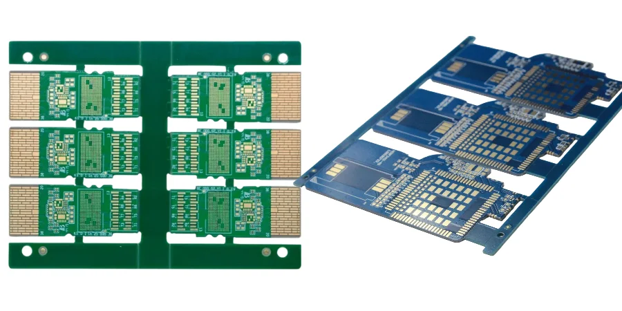
In the data-center optical-module era of 800G, 1.6T, and beyond, every design decision directly impacts performance, reliability, and cost. While SMT is the default for most components, THT/through-hole soldering remains a critical enabler in optical-module PCB design thanks to unmatched mechanical strength and specific electrical/thermal characteristics. From the cage that must withstand repeated plug/unplug stress to the power inductors that deliver stable current to high-speed laser drivers, THT execution often determines whether an optical module succeeds or fails.
From an opto-electronic co-design engineer’s perspective, this article breaks down the challenges and solutions of THT/through-hole soldering in modern optical-module PCBs. We explain how it affects high-speed SI, thermal-management efficiency, and precision alignment with optical components—and how, in demanding OSFP 800G transceiver board quick turn programs, strong THT design and manufacturing practices protect end-product performance.
The dual role of THT/through-hole soldering in optical modules: mechanical anchoring and electrical interconnect
Inside a compact optical module, THT/through-hole soldering plays a dual role that goes far beyond simple connectivity.
First, it provides mechanical anchoring. Connectors and cages for pluggable modules such as QSFP-DD and OSFP must survive thousands of insertion cycles. The mechanical stress is far beyond what SMT joints can reliably carry. By inserting leads through the PCB and soldering them, THT forms a strong mechanical lock that supports long-term connection reliability.
Second, it provides electrical and thermal interconnect. Many high-power or high-frequency filtering parts (e.g., bulk capacitors, chokes) still use THT packages for better electrical behavior and heat dissipation. But this also introduces major challenges. Under 56/112 Gbps PAM4, a THT via becomes a complex R‑L‑C network. Via stubs create reflections and impedance discontinuities; in the worst case, resonances can destroy the eye diagram. Achieving OSFP 800G transceiver board impedance control is therefore not only about microstrip/stripline—it also requires fine-grain 3D EM modeling and optimization of THT via structures.
Laser driver and TIA/LA: power delivery and isolation challenges in high-speed analog
The heart of an optical module is the Laser Driver and the TIA/LA. These high-speed analog circuits are extremely sensitive to power quality. Even small noise or droop can increase optical jitter and noise, degrading SNR. Strong Laser driver PCB quality is the foundation of module performance.
THT components play key roles in the PDN. Bulk electrolytic or tantalum capacitors often use THT packages for low-frequency filtering and energy storage at the main power entry. Their placement, via design, and connection to power planes directly impact PDN impedance. Poor THT interconnect can add extra ESL, reducing high-frequency filtering and even creating coupling paths that inject noise.
In QSFP-DD module PCB quick turn programs, fast iteration and PDN verification are critical. Engineers must use simulation tools to quantify how THT capacitor placement affects overall rail noise—and ensure that digital control circuits (MCU, CMIS controller) do not pollute the sensitive TIA/LA rails through shared THT return paths. This requires PCB manufacturers capable of producing high-precision, high-reliability multilayer PCBs with accurate partitioning and isolation of complex power/ground planes.
THT vs. SMT in key optical-module components
| Component | Preferred technique | Key benefits | Design challenges |
|---|---|---|---|
| Cage / shielding | THT/through-hole soldering | Very high mechanical strength for insertion cycles; strong EMI shielding ground. | Consumes PCB area; more complex soldering process (wave/selective). |
| Edge connector pins | THT/through-hole soldering | High mechanical stability for reliable host connection. | Via stubs hurt high-speed SI; backdrilling is often required. |
| DSP / high-speed ICs | SMT (BGA/LGA) | High-density I/O, short electrical paths, excellent signal performance. | Very high requirements for soldering quality and PCB flatness; complex thermal-stress control. |
| High-power inductors/capacitors | THT/through-hole soldering | Higher rated current, better heat dissipation, strong mechanical fixation. | Parasitic ESL can degrade high-frequency PDN performance. |
Optical interface and mechanical tolerances: co-design of MT Ferrule and THT cage
The goal of an optical module is efficient and stable electro‑optic conversion—precisely coupling laser output into fiber, and aligning fiber input onto photodiodes. This is typically done via micro-optic lens arrays and MT Ferrule interfaces. The optical sub-assembly (OSA) is fixed on the PCB and aligned to the cage and external fiber connector (e.g., MPO) that is soldered via THT.
The key is tolerance stack-up control. The THT-soldered cage provides a mechanical datum for the module; cage position accuracy affects connector-to-OSA alignment. Material selection for MT ferrule connector interface materials is also critical: the CTE must match across the PCB substrate, OSA base, and cage material. Any mismatch can cause micron-scale drift over temperature cycling—enough to reduce optical power significantly or even break the link.
Therefore, process stability and repeatability of THT/through-hole soldering is a prerequisite for optical alignment. Drill position accuracy, and post-solder positional consistency/verticality, must be tightly controlled. This demands not only high-precision drilling, but also excellent process control in through-hole assembly.
QSFP-DD/OSFP cage and thermal design: THT as a critical heat-conduction path
As module rates move to 800G and beyond, power dissipation rises to 20–25 W or more. This heat flux creates severe thermal challenges. The cage is not only EMI shielding and mechanical support—it is also a primary thermal path. Via thermal pads, it conducts heat to the host heatsink.
THT joints become a key “thermal bridge”. Cage THT pins provide mechanical fixation, and their large metal volume plus connection to large ground copper areas enable efficient heat conduction. PCB heat—especially from DSPs, drivers, and TIAs—can flow through thermal vias into internal ground layers and then out through the cage’s THT joints.
For OSFP 800G transceiver board quick turn design, thermal simulation is mandatory. Engineers must accurately model the thermal resistance of THT joints and optimize nearby thermal-via arrays to minimize total junction-to-ambient resistance. A well-designed THT thermal path reduces laser operating temperature, mitigates wavelength drift, and extends TIA lifetime—improving module reliability. This again highlights the value of a partner with strong high-speed PCB manufacturing and thermal design capability.
Core THT design points for high-speed optical modules
- Prioritize SI: For THT pins on high-speed signal paths, use backdrilling (Backdrilling) to remove unused stubs and eliminate reflection sources—this is a key step for strict `OSFP 800G transceiver board impedance control`.
- Thermal co-design: Fully connect cage THT pads to PCB ground/thermal copper and strategically place thermal via arrays to build a low-thermal-resistance path from chips to the cage.
- PDN optimization: Carefully evaluate placement and parasitic inductance of THT power parts to avoid high-frequency noise-coupling paths and sustain `Laser driver PCB quality`.
- Mechanical tolerance control: Drill accuracy and post-solder positional consistency of THT holes are foundational to optical alignment and module interoperability.
- DFM alignment: Align early with the PCB supplier (e.g., HILPCB) on THT placement to fit the process window for wave or selective soldering—critical for `QSFP-DD module PCB quick turn` success.
PAM4 channel integrity: SI/PI challenges introduced by THT and backdrilling optimization
With PAM4, each symbol carries 2 bits, but SNR margin drops sharply—systems become far more sensitive to impedance discontinuities and noise. THT structures, especially press-fit pins on edge connectors, are among the toughest problems in SI design.
When a high-speed differential signal passes through a THT via, the unused lower portion (stub) behaves like an open transmission line. At 112 Gbps (Nyquist ~28 GHz) and above, the stub can resonate at a quarter wavelength, creating deep insertion-loss notches at specific frequencies. This can collapse the eye diagram and prevent BER from converging.
The solution is backdrilling (Backdrilling / Controlled Depth Drilling). After lamination and soldering, excess plated copper is drilled out from the backside so only the conductive segment required for signal transfer remains. This shortens the stub dramatically and pushes resonances far above the signal bandwidth. Precise backdrill-depth control is a key manufacturing process for OSFP 800G transceiver board impedance control. It requires advanced equipment and strict process control to remove as much stub as possible without damaging signal layers.
Manufacturing and assembly: ensuring reliable THT/through-hole soldering
Design intent must be realized by high-quality fabrication and assembly. Reliability of THT/through-hole soldering depends on multiple process parameters:
- Hole-wall quality: Hole walls must be smooth and burr-free, with strong and uniform plated copper after PTH processing—critical for long-term electrical reliability and heat conduction.
- Soldering process: For optical-module PCBs with many SMT parts, THT is typically done via selective wave soldering or manual soldering. Tight control of the process window (temperature, time, flux activity) is essential for full, bright, void-free joints.
- Thermal-stress management: THT parts have higher thermal mass than SMT parts and can create severe local thermal shock. Use high‑Tg materials and optimized profiles to prevent delamination, blistering, or warpage.
For fast time-to-market OSFP 800G transceiver board quick turn and QSFP-DD module PCB quick turn builds, selecting a supplier that can deliver both PCB fabrication and turnkey assembly is critical. It shortens the supply chain and ensures DFM feedback is integrated early—avoiding costly rework and delays. Excellent Laser driver PCB quality is a direct result of this integrated capability.
Conclusion: mastering THT/through-hole soldering is key to winning the future
THT/through-hole soldering is far from obsolete—it remains the foundation for addressing mechanical, thermal, and selected electrical challenges in advanced data-center optical modules. While it delivers unmatched mechanical strength, it also introduces unique complexity in high-speed SI, PDN behavior, and thermal design.
From enabling tight OSFP 800G transceiver board impedance control via backdrilling, to supporting precise optical alignment alongside MT ferrule connector interface materials, to sustaining strict Laser driver PCB quality, every step requires deep understanding and disciplined process control. For engineering teams targeting leadership in the 800G/1.6T era, partnering with experts like HILPCB—who combine high-speed PCB fabrication and assembly experience—is a direct path to success.
Common Questions
Why is THT still relevant in optical module PCBs?
It is often the best choice for cages, shielding structures, power parts, and other components that need strong mechanical anchoring or robust thermal paths.
How does THT affect high-speed optical module performance?
Poorly designed through-hole transitions can damage impedance continuity and eye quality on 56G and 112G PAM4 links.
Why is backdrilling important for these boards?
It removes unused via stubs that would otherwise create reflections and resonance in very high-speed interconnect structures.
What else must be controlled besides soldering quality?
Laser-driver power quality, optical alignment accuracy, connector mechanics, and the material system around MT ferrule interfaces all matter.