
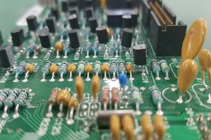
THT/through-hole soldering: managing high power density and thermal challenges in power and cooling system PCBs
In data centers, new energy vehicles, and telecom infrastructure, power density is rising at an unprecedented pace. Direct 48V→1V conversion, hundreds of amps of current, and demanding cooling requirements push PCB design and manufacturing to the limit. Even in an era dominated by SMT, a “traditional” process—THT/through-hole soldering—is returning as a core pillar for high-power power-and-cooling systems because of its mechanical robustness and strong thermal conduction. From the perspective of a high power-density power engineer, this article explains how THT/through-hole soldering addresses the triple challenge of high current, high heat flux, and high reliability.
Why THT/through-hole soldering is indispensable in high-power applications
While SMT excels in density and automation, THT’s physical characteristics are hard to replace in high-current, high-stress, heavy-component scenarios:
- Outstanding mechanical strength: leads pass through the PCB and are fully wetted, forming strong anchors. For heavy parts (large inductors, busbar connectors, large electrolytics, heatsinks), this resists vibration, shock, and thermal cycling.
- High current capacity: THT leads and plated through holes (PTH) create a low-resistance 3D path. Compared to limited SMT pad contact area, THT joints can carry tens to hundreds of amps, reducing I²R loss and local heating.
- Efficient vertical heat path: the through hole itself is a vertical thermal conduit. THT device leads (power MOSFET/IGBT) can conduct heat into internal planes, which act as built-in heat spreaders.
Power modules and VRM: THT in multiphase interleaving topologies
Modern servers and AI accelerators demand extreme VRM current (>1000A) and fast transient response. Multiphase interleaving buck converters are the mainstream topology, and THT/through-hole soldering is key:
- Input/output connectors: 48V inputs and 12V/1V outputs often use high-current THT connectors or Press-fit terminals for low impedance and reliability.
- Power inductors: each phase needs a large inductor; THT mounting provides structural stability for long operation and shipping stress.
- Bulk capacitors: input/output bulk capacitors are often THT; solid mounting is critical for transient current support.
Across NPI EVT/DVT/PVT, VRM modules undergo strict power cycling and thermal shock tests, where THT joint reliability is a key metric. A strong NPI EVT/DVT/PVT flow ensures a smooth transition from prototype to mass production.
Key metrics: THT vs SMT for high-power components
| Metric | THT/through-hole soldering | SMT (Surface-Mount Technology) |
|---|---|---|
| Current capacity | Very high (hundreds of amps) | Limited (pad area and paste volume constrained) |
| Mechanical strength | Very high, strong vibration/shock resistance | Medium, weaker for heavy parts |
| Thermal path | Vertical conduction into internal planes (efficient) | Mainly pads + thermal vias (longer path) |
| Best-fit parts | Connectors, large inductors/caps, power modules, heatsinks | ICs, resistors, MLCCs, small power devices |
PDN optimization: using THT to build low-impedance current paths
Power Distribution Network (PDN) design aims to deliver stable, clean voltage across load conditions. In high-current applications, DC resistance and AC impedance are central:
- Heavy copper / thick copper: to reduce DC resistance, we often use Heavy Copper PCB with 3 oz, 4 oz or more. THT vias connect these thick layers reliably, creating a low-impedance 3D current network.
- Busbar integration: when current exceeds what copper planes can carry, integrating a busbar on the PCB is common. THT soldering or Press-fit provides the most reliable electrical and mechanical busbar-to-PCB connection.
- Thermal via arrays: dense Thermal Via Array structures (built via THT processes) conduct heat from power devices down into large internal planes, lowering junction temperature.
Thermal management: THT as a key element in passive cooling paths
Effective thermal management is required for long-term stability. THT/through-hole soldering itself is an embedded passive heat path:
- Enhanced thermal vias: via fill with conductive material or copper filling can further reduce thermal resistance.
- Components as heat spreaders: many THT power packages (TO-220/TO-247) can be mechanically attached to external heatsinks; leads also provide additional heat flow paths into the PCB.
- Press-fit: a solderless THT interconnect that creates a gas-tight cold weld via precision hole/pin geometry. It avoids solder heat stress and provides very low contact resistance and strong thermal conduction—great for high-reliability, high-current products.
To handle harsh environments (humidity, salt fog, dust), PCBA is often protected with Conformal coating. High-quality coating protects THT joints and components without significantly degrading thermal performance.
High-power PCB thermal design workflow
- Identify heat sources and power budget: define major heat generators (VRM, MOSFET, inductors) and worst-case dissipation.
- Plan heat paths: use THT thermal vias, heavy copper planes, and [High Thermal PCB](/products/high-thermal-pcb) materials to route heat flow.
- Optimize placement: spread high heat-flux parts to avoid concentrated hot spots; use THT connectors to conduct heat into the chassis where applicable.
- Thermal simulation: evaluate and tune via count/size/placement using thermal simulation tools.
- Prototype validation: run thermal imaging during NPI EVT/DVT/PVT to validate simulation and iterate.
Manufacturing and assembly: from Selective wave soldering to First Article Inspection (FAI)
Mixed-technology (SMT + THT) PCBA is much more complex than pure SMT:
- Selective wave soldering: instead of full-board wave, a mini nozzle solders only target THT joints, protecting SMT parts and improving consistency.
- Manual touch-up: some extreme thermal-mass joints still require skilled hand soldering to achieve full fill and wetting.
- First Article Inspection (FAI): before mass production, First Article Inspection (FAI) verifies part number, polarity, insertion depth, and solder quality for every THT component to prevent systemic mistakes. A reliable Turnkey PCBA partner like HILPCB treats FAI as standard and provides a detailed report.
Reliability validation: keeping THT joints stable over the long term
High-power systems often target 10+ years of service, making reliability critical:
- Thermal cycling to evaluate fatigue cracking risk.
- Vibration/shock to validate mechanical anchoring.
- Environmental protection: Conformal coating reduces electrochemical migration/corrosion under humidity/contamination.
Co-design: making THT coexist with SMT (especially Low-void BGA reflow)
Modern high-power PCBs are complex mixed-technology systems. For example, a large BGA reflow on one side needs tight profile control. Subsequent THT soldering (Selective wave soldering) must not overheat already-reflowed BGAs. This requires thermal keep-out planning and tight parameter control. For the BGA itself, Low-void BGA reflow is essential for both thermal and electrical performance: voids increase thermal resistance and reliability risk. Choosing a Turnkey PCBA partner that can execute both Low-void BGA reflow and high-quality THT is a practical success factor.
HILPCB assembly advantage: high-power mixed technology expertise
- Advanced THT processes: Selective wave soldering, Press-fit, and robotic soldering for consistent, reliable joints.
- Precision SMT capability: focused on Low-void BGA reflow and 0201/01005 placement for high-density designs.
- Strict quality control: from First Article Inspection (FAI) to in-line AOI/X-Ray inspection.
- Value-added services: Conformal coating, potting, and Box Build for complete deliverables.
HILPCB Turnkey PCBA: one-stop solution for high-power THT/through-hole soldering
High-power PCB design and manufacturing spans materials, thermals, and manufacturing processes. A capable partner matters. HILPCB’s Turnkey PCBA service covers the full lifecycle: DFM/DFA review, sourcing, PCB fabrication, final assembly and test.
We understand the role of THT/through-hole soldering in high-power applications and integrate it seamlessly with advanced SMT processes like Low-void BGA reflow. Our NPI EVT/DVT/PVT support team works closely with you to balance performance, cost, and manufacturability. Every build starts with strict First Article Inspection (FAI), and value-added services like Conformal coating can be included as needed—delivering fully validated, plug-and-play products.
Conclusion
THT/through-hole soldering is far from obsolete. In the high power-density era, it is a foundation for managing electrical, mechanical, and thermal challenges. It provides low-impedance high-current paths, rock-solid anchoring for heavy parts, and efficient vertical thermal conduction.
For your next high-power power-delivery or cooling-system PCB, treat THT/through-hole soldering as a core design element. With an experienced partner like HILPCB, your complex design can be realized with top-tier quality and reliability.