
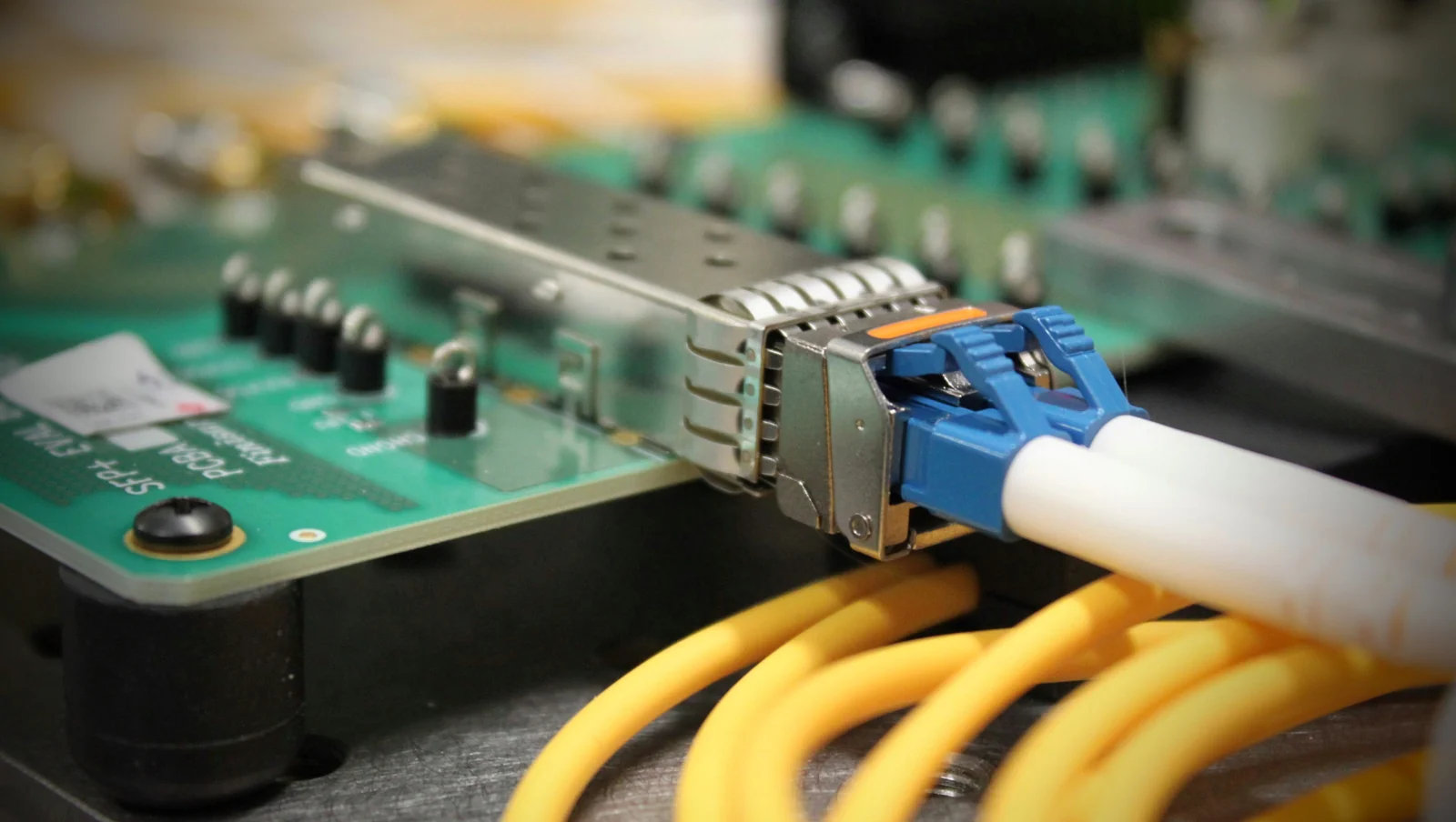
Turnkey optical module PCBA is a controlled workflow that joins component sourcing, PCB fabrication, assembly, inspection, programming, electrical bring-up, and agreed production tests for a pluggable or on-board optical transceiver. It does not transfer ownership of the optical design, form-factor compliance, firmware, host interoperability, or finished-module qualification unless those deliverables are explicitly contracted.
Key Takeaways
- Freeze the form factor, host electrical interface, media interface, lane/application map, CMIS edition, power class, thermal boundary, optical architecture, and test responsibility before releasing the PCB.
- PAM4 carries two bits per symbol but has smaller vertical decision margins than NRZ; package, launches, traces, vias, connector, crosstalk, power noise, and equalization must share one channel budget.
- Select laminate, copper profile, stackup, trace geometry, via treatment, and test coupons from the modeled channel—not from a generic “800G material” label.
- Some optical engines use thermoelectric cooling and others do not. A TEC moves heat and consumes power, so it must be included in the module and host thermal balance when present.
- Thermal vias, copper, interface materials, module shell, heat sink, contact pressure, airflow, and host cage form one path. Board-level changes cannot compensate for an undefined system boundary.
- Conventional SMT inspection cannot prove optical alignment, link BER, receiver sensitivity, or transmitter quality. Those require dedicated optoelectronic processes, instruments, firmware, fixtures, and limits.
- SPI, AOI, and X-ray provide different evidence; none guarantees solder-joint reliability by itself. Inspection coverage and acceptance criteria must be defined by package and risk.
- A turnkey supplier should release a traceable evidence package, not merely a powered board: stackup/coupon data, material and lot records, inspection results, programming identity, test data, deviations, and change history.
Contents
- What Is Included in Turnkey Optical Module PCBA?
- Which Requirements Must Be Frozen First?
- How Is the PAM4 Channel Budget Preserved?
- How Should Stackup and Fabrication Controls Be Specified?
- How Are Power and Thermal Boundaries Designed?
- How Do Warpage and Optical Alignment Affect Assembly?
- What Should SMT Inspection Actually Prove?
- How Does CMIS Change Bring-Up and Test?
- What Evidence Is Needed from Prototype to Production?
- How Should Turnkey Responsibilities Be Divided?
- What Should an Optical Module PCBA RFQ Include?
What Is Included in Turnkey Optical Module PCBA?
“Turnkey” describes an agreed supply-chain and manufacturing scope, not a performance grade. One supplier may procure approved parts, fabricate boards, assemble, inspect, program, and run customer-defined tests. Another may also manage fixtures, component lifecycle, failure analysis, optical-engine integration, enclosure assembly, or finished-module test. Compare the statement of work, not the label.
A typical optical module contains a host-edge interface, retimer or DSP where required, laser drivers, TIAs, clocking, power conversion, controller and memory, temperature and current sensing, and an optical subassembly or silicon-photonics engine. The module shell, connector, fibers, heat spreader, host cage, and switch airflow are outside the bare PCB but directly affect electrical, optical, and thermal results.
The customer design authority should supply released requirements and acceptance limits. The PCBA partner should return build evidence and control deviations. Optical-component procurement also needs explicit rules for lot traceability, handling, storage, ESD, moisture sensitivity, firmware/key provisioning, calibration data, and counterfeit avoidance.
Which Requirements Must Be Frozen First?
Requirement-to-board-and-evidence matrix
| Product input | Board/PCBA consequence | Evidence to require |
|---|---|---|
| QSFP, QSFP-DD, OSFP, on-board, or proprietary form factor | Outline, thickness, edge contacts, keepouts, cage/shell fit, low-speed pins, power classes and heat-sink interface | Controlled drawing, form-factor compliance review, fit/coplanarity records |
| Host electrical application | Lane count/rate, PAM4 or NRZ, reference clocks, equalization, connector launch, return path and crosstalk budget | End-to-end channel model, stackup, impedance/loss coupons, TDR/VNA correlation as specified |
| Optical application | Wavelengths, reach, fiber/connector, transmitter/receiver architecture, optical engine and calibration | Optical test plan, reference transmitter/receiver, power/BER or standards-specific results |
| CMIS or other management interface | Memory map, state machines, application advertisement, power modes, data-path initialization, alarms, firmware update | Register compliance, state-transition, fault, recovery and host-interoperability logs |
| Power and thermal limit | Rail tolerance/noise, inrush, sequencing, module power state, component dissipation, shell/TIM/heatsink/airflow | PDN analysis, rail tests, thermal model, hot-state measurements and protection behavior |
| Production and field life | Materials, process window, traceability, environmental stresses, change policy, repair strategy | FAI, inspection/test records, qualification allocation, control plan, PCN and deviation history |
Do not copy a previous 400G or 800G build and assume the same controls apply. Electrical lane architecture, DSP use, optics, package set, power state, host connector, material availability, and mechanical cooling can change within the same aggregate data-rate label.
How Is the PAM4 Channel Budget Preserved?
PAM4 represents four amplitude levels, so noise, loss, reflection, crosstalk, jitter, nonlinearity, and power-supply modulation consume a tighter eye than a two-level NRZ link at a comparable symbol rate. PCB impedance alone is therefore an incomplete release criterion.
Model the electrical path from the relevant package model through breakout, vias, traces, AC-coupling structures, edge fingers or connector, and the next package. Include material dielectric loss, conductor loss and roughness model, fiber-weave effects where material and geometry make them relevant, via stubs, reference transitions, connector launches, skew, aggressors, and manufacturing tolerances.
Length matching is not the objective by itself. Match within the allocated skew budget while minimizing unnecessary length and discontinuities. A tightly matched pair that is longer, crosses more layers, or uses poorly controlled vias can have less margin than a shorter pair with a small permitted mismatch.
Equalization can recover some channel loss but cannot justify unbounded discontinuities or crosstalk. Freeze which assumptions belong to the host, module DSP/retimer, transmitter, receiver, and test fixture. Correlate simulation to coupon and assembled-channel measurements before declaring the production window.
How Should Stackup and Fabrication Controls Be Specified?
Choose a high-speed PCB construction from the actual insertion-loss, impedance, skew, thickness, routing-density, thermal, assembly, availability, and cost targets. Brand names such as Megtron or Tachyon do not replace a controlled laminate designation, resin system, glass style, copper profile, pressed thickness, Dk/Df method and frequency, or approved substitute policy.
Release documentation should state:
- finished layer stackup, materials, copper type/profile and thickness, dielectric targets and tolerances
- impedance structures, geometry, reference planes, solder-mask assumption, coupon design and acceptance method
- maximum permitted via stub or backdrill controls where the channel analysis requires them
- line/space, registration, drill, annular ring, edge-finger, bevel, plating, surface finish, flatness/warpage, and dimensional requirements
- electrical test, TDR and insertion-loss test scope, cross-section or microvia evidence, data format, sampling, and record retention
A “100-ohm differential” note is insufficient if the fabricator may change glass style, copper roughness, mask, pressed dielectric, or trace width without re-modeling. Agree on an impedance-adjustment workflow and determine which changes require customer approval.
How Are Power and Thermal Boundaries Designed?
The form-factor specification and CMIS data include module power behavior, but actual dissipation depends on application, lane mode, optics, DSP, firmware, voltage, temperature, process, and traffic. Use the declared maximum and measured operating modes rather than a generic claim that every 800G or 1.6T module dissipates the same power.
Build a rail budget for input tolerance, inrush, ripple/noise, sequencing, current limit, startup, low-power state, full operation, faults, and host supply interaction. Keep switching-current loops compact and prevent DC/DC noise from modulating clocks, laser drivers, TIAs, references, and management ADCs. Test hot-plug and state transitions with the representative host impedance.
Some laser architectures use a TEC for wavelength or temperature control; others are designed for uncooled operation. When a TEC is present, its electrical input and pumped heat both reach the rejection path. TEC ripple, control stability, sensor placement, condensation assumptions, and fault behavior need system validation.
Thermal design must connect junction-to-case or board paths to copper/vias, spreader, TIM, shell, heat sink, contact pressure, cage, airflow, and ambient. A via array only moves heat to another surface. Copper balance may help fabrication and warpage, but thermal spreading and mechanical symmetry need separate analysis.
How Do Warpage and Optical Alignment Affect Assembly?
Laminate, copper, molding compound, ceramic, silicon, solder, adhesive, shell, and optical subassembly expand differently through assembly and operation. The relevant variables are the actual material properties, construction, component locations, reflow profile, fixture/support, cooling rate, and mechanical constraints—not one generic CTE table.
Board warpage can reduce BGA/LGA coplanarity, strain solder joints, shift shell contact, and disturb mechanical alignment. Define measurement condition, datum, temperature state, sampling, and limit from package and module needs. “Symmetrical stackup” is a useful starting rule but does not guarantee low warpage when copper density, component mass, cutouts, edge fingers, and local structures are asymmetric.
Optical alignment is also a separate process. Conventional pick-and-place can assemble many electronic and mechanical parts, but passive or active alignment of lasers, lenses, fiber arrays, TOSA/ROSA parts, or photonic engines may require specialist equipment, metrology, adhesives, curing, cleanliness, and live optical feedback. State whether the turnkey scope ends at electronic PCBA or includes qualified optoelectronic integration.
What Should SMT Inspection Actually Prove?
SPI measures solder-paste deposits before placement; AOI finds visible presence, polarity, alignment, and solder-appearance defects; X-ray reveals selected hidden-joint conditions. Coverage depends on package, algorithm, view, resolution, program, sample plan, and acceptance criteria. X-ray cannot prove every intermetallic or fatigue property, and an attractive image cannot prove SI or optical performance.
Define paste, stencil, placement, reflow atmosphere/profile, board support, moisture handling, cleaning, and inspection from the assembly. Void criteria must follow component guidance, thermal/electrical need, workmanship requirements, and customer specification; “void-free” is not a realistic universal process promise. Vacuum reflow is a conditional process choice, not a requirement for every optical module.
Conformal coating is similarly conditional. It can support contamination or humidity protection but can foul edge contacts, optical surfaces, connectors, calibration features, TIM areas, or rework. Specify chemistry, cleanliness, mask zones, thickness, cure, inspection, compatibility, and qualification before adding it.
How Does CMIS Change Bring-Up and Test?
OIF CMIS defines a common management interface for pluggable and on-board modules using a two-wire management link. CMIS 5.3 includes module and data-path state machines, application advertisement/selection, lane assignment, power behavior, monitoring, controls, alarms, and diagnostic functions.
Production test must use the contractually selected CMIS edition and application codes. At minimum, verify identity and revision fields, firmware, low-power and full-power transitions, application advertisement, data-path initialization, lane controls, monitors/alarms, resets, fault injection where supported, and recovery from interrupted power or communication.
CMIS register access is not complete functional validation. A module can answer management commands while a high-speed lane, optical path, calibration table, thermal sensor, or power rail is wrong. Keep management, electrical data-path, optical, thermal, and environmental evidence separate, then link them by serial number and firmware version.
What Evidence Is Needed from Prototype to Production?
Optical module NPI release gate
| Gate | Evidence before release |
|---|---|
| Design baseline | Controlled schematic/BOM/layout, stackup, channel and PDN assumptions, mechanical/thermal model, firmware and test revisions |
| Fabrication | Material and stackup records, impedance/loss results as specified, electrical test, cross-section/microvia evidence, dimensions and warpage |
| Assembly | Paste/reflow records, SPI/AOI/X-ray results, moisture/ESD controls, deviations, component and optical-part traceability |
| Electrical bring-up | Rail sequence/noise, current, reset/clock, controller access, CMIS states, data-path continuity and fault behavior |
| Performance correlation | Host/module channel data, hot-state SI/BER test, thermal map, optical measurements, calibration and interoperability as allocated |
| Production readiness | Approved fixtures/software/limits, gauge correlation, golden references, yield/failure codes, repair rules, serial data and change triggers |
One passing sample proves feasibility, not process capability. Pilot builds should expose material lots, panel positions, reflow loads, operators/lines, fixtures, temperatures, and relevant component variation. Review distributions and failure signatures rather than reporting only pass/fail totals.
How Should Turnkey Responsibilities Be Divided?
| Deliverable | Typical design-authority responsibility | Typical PCB/PCBA responsibility |
|---|---|---|
| Electrical/optical architecture | Form factor, application, channel budget, optics, firmware, calibration and compliance requirements | DFM/DFA feedback and manufacture to released data |
| PCB performance | Models, limits, coupons, stackup approval and change authority | Fabrication process, material control, coupons/tests and traceable records |
| Assembly | Package requirements, critical features, workmanship/test limits | Process development, assembly, inspection, deviations and corrective action |
| Optoelectronic integration | Alignment method, optical limits, qualified equipment and process ownership | Only if explicitly within demonstrated and contracted capability |
| Finished-module validation | Host interoperability, CMIS/application, BER, optical, thermal, safety/EMC and reliability qualification | Customer-defined production tests using approved fixtures, software and limits |
HILPCB can support turnkey sourcing, PCB fabrication, SMT assembly, process inspection, programming and agreed board/PCBA tests. The quotation must identify which optical parts, alignment, calibration, high-speed fixtures, BER instruments, optical equipment, licensed firmware, host platforms, and qualification tests are customer-supplied or separately scoped.
What Should an Optical Module PCBA RFQ Include?
Product and design baseline
- form factor/specification edition, application/lane map, aggregate rate, host electrical interface, optical reach/media, CMIS edition, power class and environmental use
- released schematic, BOM/AVL, fabrication and assembly data, stackup, impedance/loss table, mechanical model, thermal boundary, firmware, programming and calibration files
Fabrication and assembly controls
- approved laminate/copper and substitutions, via/backdrill, edge fingers, finish, coupons/tests, dimensions, warpage, panel, traceability and change-control requirements
- package list, MSL/ESD/cleanliness controls, stencil/reflow, support fixtures, SPI/AOI/X-ray coverage, void criteria, coating/masking and optoelectronic integration boundary
Test and release evidence
- rail, clock/reset, CMIS, data-path, BER, optical, thermal, interoperability and environmental test ownership
- fixtures, cables, host platforms, instruments, reference modules, software/firmware, calibration, limits, sample plan, raw-data retention, failure analysis and requalification triggers
Commercial and lifecycle
- prototype/pilot/volume quantities, forecast, approved sources, long-lead/NCNR parts, excess ownership, lead time, lot/date-code rules, PCN/PDN handling, spares and repair policy
Without these inputs, “turnkey 800G optical module PCBA” is not a quote-ready specification.
Reference Standards and Specifications
- OIF-CMIS-05.3 — Optical Internetworking Forum
- IEEE 802.3 and IEEE 802.3ck — IEEE
- SFF-8679 and SFF-8636 — SNIA SFF Technology Affiliate
- QSFP-DD Hardware Specification — QSFP-DD MSA
- OSFP Specification — OSFP MSA
- IPC-2221, IPC-6012 and IPC-TM-650 — IPC
- J-STD-001 and IPC-A-610 — IPC
The contract must identify applicable editions, form-factor documents, optical/Ethernet application standards, customer limits, and precedence. Standards compliance applies to the defined module/system evidence, not automatically to a bare PCB or assembly.
Frequently Asked Questions
Does every 800G optical module use the same PCB stackup?
No. Stackup depends on lane architecture, channel length, packages, loss budget, form factor, density, power, manufacturing capability, and cost. Select it through modeling and fabrication correlation.
Are thermal vias enough to cool an optical module?
No. They transfer heat between board surfaces. The complete path also needs component interfaces, copper, spreader or shell, TIM, contact pressure, heat sink, cage, airflow, and ambient assumptions.
Do all optical modules require a TEC?
No. TEC use depends on laser/optical architecture and wavelength-control requirements. When used, include TEC power, pumped heat, control stability, sensing, and fault behavior in the system budget.
Can SPI, AOI, and X-ray prove module performance?
They prove selected process and assembly attributes. They do not prove high-speed channel margin, BER, optical power, receiver performance, CMIS behavior, calibration, thermal stability, or host interoperability.
What is the most important turnkey PCBA handoff?
The controlled requirement-and-evidence matrix is the key handoff. It ties each form-factor, electrical, thermal, optical, firmware, manufacturing, and test requirement to an owner, method, limit, record, and change trigger.
Can HILPCB deliver a finished, certified optical module?
Only a project-specific statement of work can define that scope. HILPCB can quote PCB and PCBA services plus agreed tests; optical integration, licensed firmware, host interoperability and finished-module qualification require explicit equipment, methods, limits, and responsibility.
Release a Repeatable Module, Not One Good Sample
Turnkey optical module PCBA succeeds when high-speed, power, thermal, mechanical, firmware, optical, sourcing, and test assumptions become one controlled production baseline. The supplier must be able to show what was built, how it was measured, which deviations were accepted, and when a change requires renewed evidence.
Send HILPCB the release package and responsibility matrix for a scoped turnkey assembly review. The resulting quote can separate PCB/PCBA deliverables from specialist optical and system validation while preserving the evidence needed for production decisions.