
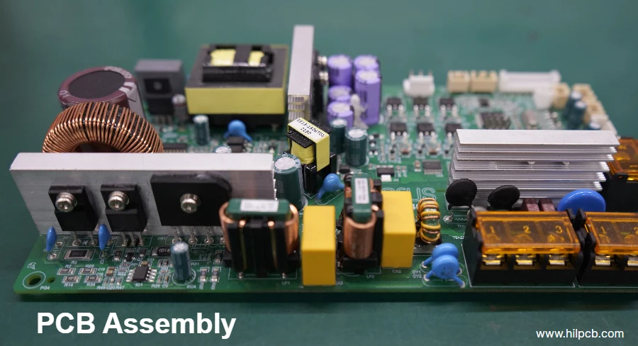
With the rapid rise of AI and HPC, Chiplet architectures and 2.5D/3D heterogeneous integration have become a key path to push beyond the physical limits of Moore’s Law. But the complexity is not only in silicon—it extends to the high-density interconnect substrates and system-level PCB that carry these advanced devices. Turning a concept into a product requires an integrated manufacturing flow that is fast, reliable, and tightly coordinated. This is exactly where Turnkey PCBA becomes strategic: a seamless solution spanning design validation, sourcing, PCB fabrication, assembly, and test—built for the packaging and interconnect challenges of the AI era.
As system architects, we know AI success depends not only on compute cores, but also on the fundamentals below: signal integrity of interconnects, stability of the power distribution network, and thermal efficiency. A tiny manufacturing defect or design oversight can degrade performance—or fail an expensive system altogether. Choosing a partner that truly understands these constraints is the foundation of success. Professional Turnkey PCBA integrates the supply chain, optimizes production, and front-loads risk assessment—so every step from prototype to mass production stays controlled and predictable.
What is the core value of Turnkey PCBA in AI systems?
Traditional PCBA often spans multiple vendors: one for PCB fabrication, another for sourcing, and another for assembly. That fragmented model may work for standard consumer products, but it is high-risk for highly integrated AI systems. AI substrates and motherboards often use very high layer-count HDI PCB, micron-level trace/space, and critical interfaces such as HBM and high-speed SerDes. Any communication gap or inconsistent standard between vendors can lead to catastrophic outcomes.
Turnkey PCBA consolidates the full value chain under a single accountable owner, delivering value through:
- Simplified supply chain management: customers interface with one supplier, dramatically reducing coordination cost and complexity. From Gerbers to finished goods, one team orchestrates the full flow for speed and accuracy.
- Front-loaded risk prevention: a professional provider performs a comprehensive DFM/DFT/DFA review before build. For AI systems, this is critical to catch design risks, material compatibility issues, and assembly challenges early.
- Faster time-to-market: fabrication, sourcing, and assembly run in parallel with tight coordination, shortening the overall schedule—vital in competitive AI markets.
- Optimized total cost of ownership (TCO): even if line-item pricing isn’t the lowest, reduced overhead, less rework/scrap, and scale purchasing power often lowers total project cost.
For AI platforms, this means the entire flow—from complex IC substrate fabrication, to precision SMT assembly, to strict final testing—operates under one unified quality system to ensure high reliability and performance.
Why DFM/DFT/DFA review is the foundation of AI PCBA success
AI substrate and system-board design pushes for extreme performance—often at the edge of manufacturing capability. For example, to enable ultra-short interconnect between HBM and SoC, you may need multiple RDL layers and tens of thousands of Microvias on an IC Substrate PCB. Theoretical performance can be excellent, but without manufacturable constraints it becomes “paper design.”
That’s where DFM/DFT/DFA review matters. It is not just a basic Gerber check—it is a deep co-optimization between design intent and production reality:
- DFM (Design for Manufacturability): focuses on PCB manufacturability—minimum trace/space vs. yield, Microvia stacking strategy (Stacked vs. Staggered), copper pillar pad design, lamination parameters for advanced materials such as ABF, and more. A strong DFM review balances performance and cost and avoids yield collapse from over-design.
- DFT (Design for Testability): ensures the PCB can be tested effectively after manufacturing. With dense BGA/connectors, DFT review recommends test-point placement, plans Flying probe test or ICT probe access, and protects 100% coverage for critical nets.
- DFA (Design for Assembly): focuses on assembly—component spacing for SMT assembly and reflow, soldering approach for dense connectors (e.g., whether Selective wave soldering is needed), and whether large thermal pads under big ICs risk voiding (Voiding), etc.
Highleap PCB Factory (HILPCB) treats DFM/DFT/DFA review as the starting point and core of Turnkey PCBA. Early involvement helps customers identify and correct risks before costly tooling changes and production delays—turning AI boards from drawings into hardware efficiently.
🌟 Turnkey PCBA: end-to-end value chain
From concept review to global delivery, HILPCB vertically integrates the supply chain to shorten NPI cycles and reduce hidden management costs.
Deep DFM/DFT review to optimize dense routing and test-point coverage—locking volume yield from the design stage.
Supply-chain control via SAP—EOL alerts plus 100% authentic procurement and lot traceability.
Supports multilayer HDI, ultra-thick copper, and high-frequency materials—meeting strict electrical performance needs in AI, communications, and industrial control.
Fully automated high-precision SMT plus nitrogen-protected selective soldering—supporting 03015/01005 placement and complex system integration.
Covers SPI/3D AOI/AXI and customized FCT—100% scenario-based testing for near-zero-defect shipment.
Professional ESD packaging plus flexible DDP/DAP logistics, backed by responsive technical support and RMA management.
How SMT assembly addresses Chiplet and SiP challenges
As AI moves toward Chiplet and SiP (System in Package), assembly faces new challenges. Traditional SMT assembly must evolve for miniaturized, high-density devices.
First is placement accuracy. SoC and HBM modules on AI accelerator cards often use large BGA or LGA packages with extremely fine pitch (down to 0.35 mm or below). This demands top-tier vision systems and placement precision—tiny rotation/offset errors can cause widespread bridging or opens. High-precision pick-and-place machines with high-resolution cameras and advanced closed-loop control are mandatory.
Second is reflow process control. AI boards are typically large, high-layer-count, thick-copper designs with high and uneven thermal mass. The same board may include a massive SoC and tiny 01005 capacitors. Building a profile that fully wets BGA balls without damaging nearby heat-sensitive parts requires multi-zone ovens and experienced process engineers—validated through repeated thermocouple trials.
Third is Underfill and Edge Bonding. For large BGA, epoxy Underfill is often used to manage stress from thermal cycling and mechanical shock. The process requires precise control of dispense volume and cure profile to avoid bubbles or incomplete fill.
HILPCB’s SMT assembly line is built for these challenges, combining leading placement/soldering equipment with an engineering team experienced in complex package assembly—delivering consistent AI product quality.
How to choose the right soldering technology for high-density AI boards
Modern AI system boards are highly integrated hybrid-technology products. Many components are reflowed SMDs, but some Through-hole parts remain irreplaceable—high-current power connectors, board-to-board high-speed connectors, or custom thermal modules. The key challenge in Turnkey PCBA is soldering these through-hole parts efficiently and reliably without damaging already-mounted dense SMT parts.
Manual soldering is flexible but inconsistent and unsuitable for volume. Traditional wave soldering indiscriminately heats the entire PCB underside; for double-sided AI boards packed with SMT parts, it can be destructive—causing bottom-side parts to drop or be damaged.
That’s why Selective wave soldering matters. A small, precisely controlled nozzle creates a mini wave to locally heat and solder only the targeted through-hole pins. Benefits include:
- Precision: solders only the target region, with minimal thermal impact to nearby SMT parts.
- Flexibility: programmable nozzle paths, dwell time, and wave height support complex pin patterns.
- High quality: tightly controlled parameters produce consistent, full fillets—better than hand soldering.
- Automation: the process is machine-driven, improving throughput and yield.
For AI accelerators with dense BGA plus high-power through-hole connectors, Selective wave soldering is indispensable for electrical integrity and long-term reliability—and a key marker of high-end Turnkey PCBA capability.
💎 HILPCB one-stop PCBA assembly core path
A digital supply chain plus a high-precision process loop to shorten your NPI cycle from prototype to delivery.
Deep DFM/DFA analysis to prevent soldering and assembly conflicts.
Global supply network with 100% authentic procurement and lot traceability.
High-precision nitrogen SMT and Selective wave soldering.
AOI, X-Ray, and flying probe test to ensure 100% qualified output.
ESD vacuum packaging and fast global logistics.
How advanced test protocols ensure final product quality
For AI accelerator cards worth tens of thousands of dollars, any field failure is unacceptable. That’s why the end of the Turnkey PCBA flow requires a strict, comprehensive test strategy to ensure every delivered unit is functional and meets performance targets.
AOI (Automated Optical Inspection): after SMT reflow, AOI scans each PCBA and compares to design data to detect assembly defects such as offset, wrong/missing parts, polarity issues, and bridging—forming the first quality gate.
AXI (X-ray inspection): for bottom-terminated packages such as BGA/LGA/QFN, joints cannot be verified optically. X-ray reveals ball shape/size/alignment and detects voiding or shorts. For critical AI devices, 100% X-ray inspection is standard.
Flying probe test: in prototype and low-volume phases, expensive ICT fixtures are not economical. Flying probe test uses fast-moving probes to contact test points/vias/pins, measure R/C/L, and check for opens/shorts—without dedicated fixtures. It is ideal for high-mix, low-volume and helps validate connectivity during NPI.
FCT (Functional test): the highest-level test simulates real operating conditions to validate full functionality. For AI accelerators, this may include power-on self-test, firmware loading, diagnostics, benchmark workloads (e.g., matrix compute), and monitoring power and temperature under varying loads.
A mature Turnkey PCBA supplier like HILPCB combines these methods based on product complexity and requirements—building a multi-layer test system from appearance to electrical to functional, intercepting defects as early as possible.
Special applications of Potting/encapsulation in AI systems
While Potting/encapsulation is traditionally used to protect circuits from harsh environments (moisture, vibration, chemicals), it is increasingly important in precision AI systems—especially for structural reinforcement and thermal management.
Structural reinforcement and stress relief Some AI subsystems—on-board optical transceivers or high-frequency connectors—are sensitive to mechanical stress. Vibration and shock during shipping/installation/operation can cause solder fatigue cracking. Local Potting/encapsulation around these components can fix them in place and distribute stress, improving mechanical reliability. Material selection (often flexible epoxy or silicone with low Young’s modulus) is critical to avoid introducing new stress during thermal expansion/contraction.
Thermal enhancement In compact AI edge devices, thermal headroom is limited. Thermally conductive potting compounds can be very effective: encapsulating hot power parts (MOSFET, DrMOS) and conducting heat into a metal enclosure or heatsink provides an efficient passive cooling path—while also improving insulation and moisture resistance.
In Turnkey PCBA, Potting/encapsulation is a tightly controlled process requiring correct resin selection, mix ratio, de-foaming, dispensing paths, and cure profiles. Mistakes can cause under-cure, internal bubbles, or destructive stress on components.
HILPCB advanced manufacturing capability snapshot
| Parameter | Spec | Why it matters for AI |
|---|---|---|
| Max layer count | 56 layers | Supports complex high-speed routing and power partitioning |
| Min trace/space | 2/2 mil (50/50 µm) | Meets dense BGA fanout and differential-pair routing needs |
| HDI structure | Anylayer interconnect | Maximizes routing space and shortens critical signal paths |
| Supported materials | Megtron 6, Tachyon, ABF | Preserves PCIe 5.0/6.0, CXL, and other high-speed signal integrity |
| Impedance control accuracy | ±5% | Reduces reflection/crosstalk and protects high-speed link quality |
How to manage the complex AI PCBA supply chain
AI BOMs often include hundreds to thousands of parts sourced globally—standard passives plus long-lead-time FPGA, custom connectors, thermal materials, and advanced laminates. Managing this complexity is a major challenge—and a key differentiator for Turnkey PCBA providers.
A strong Turnkey supplier like Highleap PCB Factory (HILPCB) builds robust supply-chain systems:
- Qualified supplier network: long-term relationships with authorized distributors and manufacturers to prevent counterfeit components.
- Risk procurement strategy: for long-lead or unstable parts, procure ahead based on customer forecasts or validate alternates.
- Traceability management: barcode traceability from receiving and kitting through assembly and shipping to quickly isolate lots if issues occur.
- Cost optimization: leverage volume purchasing to negotiate better pricing and reduce overall BOM cost.
With professional supply-chain management, Turnkey PCBA frees customers from purchasing expediting and inventory burden—so teams can focus on core algorithms and system architecture.
FAQ
What is the main value of Turnkey PCBA for AI hardware teams?
The main value is integration. Turnkey PCBA combines fabrication, sourcing, assembly, testing, and quality control into one managed flow, which reduces handoff risk and shortens the path from prototype to production.
Why is DFM/DFT/DFA review foundational in AI PCBA programs?
AI boards have dense layouts, sensitive high-speed links, complex thermal demands, and expensive components. Early DFM/DFT/DFA review helps remove manufacturability, testability, and assembly risks before they become schedule delays or yield losses.
Why do advanced test protocols matter so much in turnkey AI assembly?
AI hardware cannot rely on basic continuity checks alone. Layered test methods such as AOI, AXI, flying probe, and FCT help catch visual, electrical, and functional defects at different stages, which is critical for high-value systems.
Why is supply chain management a core part of turnkey PCBA success?
AI BOMs often include long-lead, high-cost, and hard-to-replace components. Strong supply chain control reduces counterfeit risk, stabilizes delivery, improves traceability, and helps engineering teams avoid being blocked by procurement complexity.
Conclusion: Turnkey PCBA is a strategic engine for faster AI innovation
From micro-scale copper pillar interconnects to system-level integration, AI hardware realization is a complex, cross-domain engineering effort. In this chain, manufacturing and assembly reliability, efficiency, and coordination directly determine product success. Turnkey PCBA addresses this with an end-to-end, highly integrated solution.
It front-loads risk with DFM/DFT/DFA review, protects assembly quality with precision SMT assembly and Selective wave soldering, ensures electrical performance via multiple test layers such as Flying probe test, and improves reliability in harsh environments via processes like Potting/encapsulation. Just as importantly, it simplifies supply-chain complexity so innovative teams can stay focused on their core strengths.
Choosing an experienced, technology-leading partner like HILPCB means choosing an ally that understands the unique needs of AI systems. We deliver not only assembled circuit boards, but a fully optimized, quality-controlled solution that accelerates your time-to-market. On the road to the AI future, a strong and reliable Turnkey PCBA partner is an essential engine.