
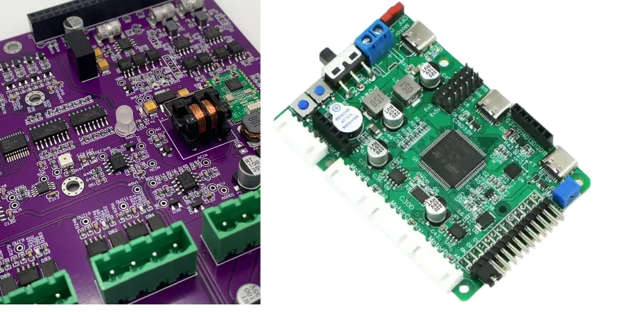
Industrial robots are a backbone of modern manufacturing. At the heart of every controller sits a PCB that must deliver precise, real-time, and safe operation. These control boards not only handle high-speed data streams and powerful motor-drive signals; they also must remain rock-solid in harsh industrial environments filled with EMI, vibration, and temperature/humidity variation. To manage these complex constraints, more teams are adopting a one-stop Turnkey PCBA model. By integrating design, sourcing, manufacturing, test, and compliance into one coordinated flow, it reduces multi-vendor risk and schedule friction—providing a dependable foundation for high-performance industrial robot control systems.
As a test & certification engineer focused on ICT/FCT, CE compliance, and coating processes, I know that industrial robot control PCB development is far more than circuit design. It is a system engineering effort spanning testability, regulatory compliance, environmental robustness, and mass-production consistency. A successful Turnkey PCBA project must account for these factors from day one and drive a rigorous DFM/DFT/DFA review—so the design is not only functional, but also manufacturable, testable, and maintainable. This article explains how the Turnkey PCBA model systematically addresses the key challenges industrial robot control PCB faces across testing, certification, protection, and production ramp.
Design for testability (DFT): building quality from the start
In complex industrial robot control PCB programs, DFT is not a late-stage patch—it is a decisive factor for success, cost, and yield. The core of DFT is to “design in” test-friendly structures and functions early, so defects can be found quickly and accurately on the line. In a complete Turnkey PCBA workflow, DFT is one of the most important early steps because it directly determines ICT/FCT coverage and diagnostic efficiency.
Test points, interfaces, and diagnostic strategy
DFT starts with careful test-point planning. These physical touch points are the bridge between ATE and the PCB. Key DFT considerations include:
Test points (Test Points):
- Accessibility: Place test points on one side of the PCB to simplify bed-of-nails access and avoid the cost/complexity of dual-side probing.
- Size and pitch: A common guideline is a pad diameter ≥ 0.8 mm and a pitch ≥ 1.27 mm to ensure stable, reliable probe contact.
- Coverage: Break out critical nets—power rails, clocks, reset, and major buses. For packages like BGA that are hard to probe, plan dedicated breakout test points.
Test interfaces (Test Interfaces):
- JTAG/Boundary Scan: For control boards with complex digital ICs (FPGA, MCU, DSP), a JTAG interface is essential. It enables pin access and interconnect tests (opens/shorts) and basic device checks without physical probes—dramatically improving coverage on dense packages.
- Debug ports: Reserve UART, SPI, or I2C ports to support firmware programming and parameter configuration in FCT, and to simplify later diagnosis and rework.
Segmented testing and diagnostics (Segmented Testing):
- Industrial robot control boards typically contain multiple functional blocks—power management, compute core, communication interfaces (Ethernet, CAN), motor drive, and sensor acquisition. By adding jumpers, 0-ohm resistors, or controllable power switches, you can electrically isolate modules. This “divide and conquer” approach lets you power and test modules independently and quickly narrow faults to a specific block—greatly improving debug efficiency.
At HILPCB, we insist on a thorough DFM/DFT/DFA review at the beginning of every Turnkey PCBA program. Our engineering team works closely with customers to review schematics and layout, and to provide actionable DFT recommendations—so the design enters production with strong testability and a solid foundation for mass production and quality control.
ICT/FCT: key points for coverage and fixture design
In PCBA manufacturing, test is the core gate that validates quality and ensures conformance to the design intent. For industrial robot control boards, ICT (in-circuit test) and FCT (functional test) are indispensable quality checkpoints—covering electrical integrity and real-world functional behavior from different angles.
ICT (In-Circuit Test): a “screen” for microscopic defects
ICT is mainly used to catch component-level manufacturing defects. Using a high-density probe array (bed-of-nails) to contact DFT test points, it measures component values (R/C/L) and detects opens, shorts, wrong parts, missing parts, and solder issues.
- Test coverage: The key to ICT is maximizing coverage, which depends directly on early DFT. A strong DFT plan can enable 95%+ component/net coverage.
- Fixture: An ICT fixture is a precision, PCB-specific tool. Its design must consider probe type (e.g., sharp/crown tips), force, lifetime, and accurate PCB alignment. For complex boards such as HDI PCB, fixture accuracy requirements are especially high. Durability also matters: in volume production, high-quality probes and robust mechanics keep performance stable over tens of thousands of cycles.
FCT (Functional Test): a “touchstone” for system performance
If ICT answers “are the parts and interconnects correct?”, FCT answers “does the system work?”. FCT validates functions by simulating the real operating environment of the PCBA.
- Simulate real operating conditions: For robot controllers, the FCT fixture must emulate input signals (encoder feedback, sensor data) and monitor outputs (motor-drive PWM waveforms, bus protocol packets). It may need a real motor load or an electronic load to verify stability and response under high current.
- Custom test tooling: FCT setups are highly customized, integrating power supplies, signal generators, oscilloscopes, DAQ cards, and host software. The design must support automation while ensuring accuracy and repeatability.
- First Article Inspection (FAI): Before volume production, First Article Inspection (FAI) is critical. FCT results from the first unit are recorded and analyzed to validate the test plan and process stability. With First Article Inspection (FAI), you ensure every production unit matches the validated “golden sample.”
A mature Turnkey PCBA supplier not only builds high-quality PCBA, but also provides an end-to-end solution—from DFT analysis to ICT/FCT fixture development and test-program implementation—so the product meets top standards from the micro level to the system level.
🤖 End-to-end test system for industrial robot control boards
From design intent to system integration, multi-dimensional inspection ensures high-reliability operation in complex industrial environments.
Optimize test-point placement and probe coverage in design to ensure critical nodes are measurable in volume production.
Digitally verify first-article BOM and placement process, confirm solder-paste wetting and component polarity, and lock the process baseline.
Use a bed-of-nails fixture for milliohm-level R/C checks to efficiently screen shorts, wrong parts, and cold solder—core process defects.
Simulate full-load robot scenarios to validate motion control algorithms, bus communications, and sensor readout logic.
Run long-duration, full-load operation at elevated temperature to expose early-life failure risks and ensure long-term stability.
Common CE/EMC certification issues and mitigation path
For industrial robot products sold into Europe, the CE mark is mandatory market access. Within CE, EMC is one of the most technically challenging and failure-prone parts. EMC requires equipment to operate normally in electromagnetic environments while not generating excessive disturbance to other devices. Industrial robot control boards—combining high-speed processors, high-power drives, and multiple interfaces—are often an EMC “hot zone.”
Common blockers in EMC testing
- Radiated emissions (RE) over limit: the most common issue. High-speed lines (DDR, LVDS), SMPS switching nodes, and clock circuits are major radiators. Poor PCB layout—signals crossing plane splits, large ground loops—turns structures into antennas that radiate noise.
- Conducted emissions (CE) over limit: noise couples through power lines into the mains. A common source is the SMPS input stage, requiring effective EMI filtering.
- ESD immunity failures: static discharge from operators can inject via ports and buttons, damaging ICs or causing resets.
- Radiated susceptibility (RS) weakness: external fields (walkie-talkies, VFDs) can trigger malfunctions—often due to insufficient shielding or noise-sensitive internal circuits.
A systematic EMC mitigation workflow
If EMC issues surface during certification, rework costs and schedule pressure spike. An experienced Turnkey PCBA partner can eliminate most EMC risks during the design phase.
- Prevention in the design phase:
- Schematic planning: reserve footprints for filters, ferrite beads, and TVS at key interfaces (power, high-speed). Even if not populated initially, they make later mitigation far easier.
- PCB layout: the core of EMC. Key tactics include: keep ground planes continuous; avoid routing signals across splits; use impedance control and differential routing for high-speed; physically isolate and partition sensitive circuits (analog sensing) from noise sources (SMPS, motor drive); use multilayer PCB with internal ground planes for better shielding.
- Pre-compliance debug and fixes: before formal testing, pre-compliance is a low-cost way to detect issues early. With a spectrum analyzer and near-field probes, you can identify sources and coupling paths. Common fixes include:
- Filtering: add/optimize common-mode chokes and X/Y capacitors at power entry.
- Shielding: add metal shields over key ICs or the whole PCBA, or use conductive gaskets to improve enclosure shielding.
- Grounding: ensure all shields and metal housings have low-impedance ground connections.
- Verification in NPI EVT/DVT/PVT: EMC validation should be built into NPI EVT/DVT/PVT. Testing and optimizing across stages helps ensure stable EMC performance in mass production.
By integrating EMC design and test services into the Turnkey PCBA workflow, HILPCB helps customers control risk from the start, pass certification smoothly, and accelerate time-to-market.
Coating and environmental protection: materials and process window
Industrial environments are harsh—dust, moisture, corrosive gases, and salt spray can severely threaten long-term PCBA reliability. To protect sensitive components and circuits, robust protection is required. Basic “three-proof” needs include moisture resistance, salt-spray resistance, and mold resistance. The two most mainstream processes are Conformal coating and Potting/encapsulation.
Conformal coating: lightweight, full-coverage protection
Conformal coating applies a thin, uniform, transparent polymer film (typically 25–75 μm) over the PCBA, closely following the contours of components and solder joints.
Material selection:
- Acrylic: low cost, easy to apply and rework, but average chemical and abrasion resistance.
- Silicone: excellent high/low temperature performance and flexibility; buffers mechanical stress and vibration, but can be sensitive to some solvents.
- Urethane: strong chemical and wear resistance, but difficult to rework.
- Parylene: vapor-deposited; extremely uniform, dense, pinhole-free, and offers the best protection—but with higher cost and process complexity.
- The right Conformal coating depends on the robot’s environment and cost target.
Process window: high-quality coating requires tight control of the “process window”—viscosity, spray/dip speed, cure temperature, and cure time. Poor control can cause bubbles, orange peel, and thickness variation that degrade protection. Automated selective coating systems can precisely control coverage and thickness while keeping “no-coat areas” (connectors, test points) clean.
Potting/encapsulation: heavy-duty, ultimate protection
For extreme shock/vibration or full waterproof/chemical resistance, Potting/encapsulation provides a higher protection level by fully encapsulating all or part of the PCBA using epoxy, urethane, or silicone.
- Benefits: unmatched mechanical strength and environmental protection; can also aid heat dissipation (thermally conductive potting) and electrical insulation.
- Challenges: Potting/encapsulation increases weight and volume; cured material is hard to remove (rework is nearly impossible); cure shrinkage/stress can damage sensitive parts. A detailed evaluation is required before committing to a potting strategy.
Whether Conformal coating or Potting/encapsulation, both are key value-added steps in Turnkey PCBA services—ensuring reliable operation over the intended lifecycle.
Protection process selection checklist
- Environment assessment:Analyze the robot’s operating environment and identify the main threats—moisture, dust, chemicals, or mechanical vibration.
- Rework requirements:If in-field rework is likely, prioritize removable Conformal Coating materials (e.g., Acrylic).
- Thermal considerations:For high-heat boards such as [Heavy copper PCB](/products/heavy-copper-pcb), choose high-thermal-conductivity potting compounds and ensure thermal paths remain effective.
- Cost budget:Parylene coating and potting can be costly; balance protection performance and project budget.
- Process validation:Before volume production, validate the selected protection process to ensure it does not negatively impact PCBA performance.
NPI and mass production: consistency, traceability, and data-driven quality
The jump from prototypes to thousands (or more) units is the final—and most critical—step for industrial robot controller projects. The challenge is ensuring every production PCBA matches the quality and performance of the thoroughly validated prototype. This requires a structured NPI flow and a strong mass-production quality system.
NPI EVT/DVT/PVT: the staircase from blueprint to reality
NPI (New Product Introduction) reduces ramp risk through staged validation.
- EVT (Engineering Validation Test): focuses on basic functional realization. Typically uses prototype PCBA to validate design concepts and resolve major circuit/firmware issues.
- DVT (Design Validation Test): aims to freeze the hardware design. PCBA is built with near-final processes and undergoes comprehensive functional, performance, safety, and EMC tests. Required hardware changes are completed here.
- PVT (Production Validation Test): the last sprint before mass production. Uses the final line, tooling, and test flow for a small pilot run to validate process stability, yield, and efficiency. First Article Inspection (FAI) is a core PVT activity to ensure first builds fully meet the design spec.
A rigorous NPI EVT/DVT/PVT process is fundamental to product maturity and manufacturability—and a signature capability of professional Turnkey PCBA suppliers.
Consistency, traceability, and data-driven quality
In mass production, the focus shifts from “can we build it?” to “can we build it consistently and well?”
Consistency:
- Strict process control: from SMT placement parameters and reflow profiles to wave-solder settings—every detail must be standardized and executed.
- Supply-chain management: ensure all component lots come from qualified suppliers with IQC. For critical components, lot locking may be required.
Traceability:
- For safety-critical industrial robots, traceability is essential. Every PCBA should have a unique serial number (barcode/QR). With it, you can trace build date, line, component lots, operators for key steps, and all test data (ICT, FCT).
- If a field issue occurs, a strong traceability system enables fast scoping and precise recall/repair—minimizing losses.
Data-driven quality management:
- Throughout Turnkey assembly, collecting and analyzing test data drives continuous improvement. With SPC monitoring ICT/FCT yield and defect distribution, anomalies can be detected early. For example, if solder-defect rates rise for a component, the system can alert engineers to inspect the placement machine or solder-paste printing process before the issue escalates.
Conclusion
Industrial robot control PCB development is a highly complex system project. Success depends not only on strong circuit design, but also on manufacturing, testing, certification, and quality management across the product lifecycle. The Turnkey PCBA model consolidates these disciplines into a unified, efficient delivery platform—providing a practical path to meet real-time performance, safety redundancy, and long-term reliability.
From early DFM/DFT/DFA review that establishes testability, to ICT/FCT and precision fixtures that guarantee electrical and functional performance; from proactive EMC design that reduces certification risk, to Conformal coating or Potting/encapsulation that boosts environmental robustness; and finally to rigorous NPI EVT/DVT/PVT plus data-driven production control for consistent, traceable output—every link matters. Choosing an experienced, full-capability Turnkey PCBA partner like HILPCB means you gain not just a high-quality board, but a team that can manage complexity from design through mass production—helping your industrial robot products win in a competitive market.
Common Questions
Why does industrial robot control hardware benefit from turnkey PCBA?
It combines design review, sourcing, manufacturing, test, and compliance work into one coordinated process for complex control boards.
What tests are most important in this type of project?
ICT, FCT, fixture strategy, and staged EVT, DVT, and PVT validation are key for proving function and manufacturing consistency.
Why are EMC and protective coatings part of the discussion?
Industrial environments expose boards to EMI, dust, moisture, and vibration, so compliance design and environmental protection are essential.
What should teams expect from a strong turnkey partner?
They should expect early DFM, DFT, and DFA input, reliable process control, and support from prototype builds through mass production.