
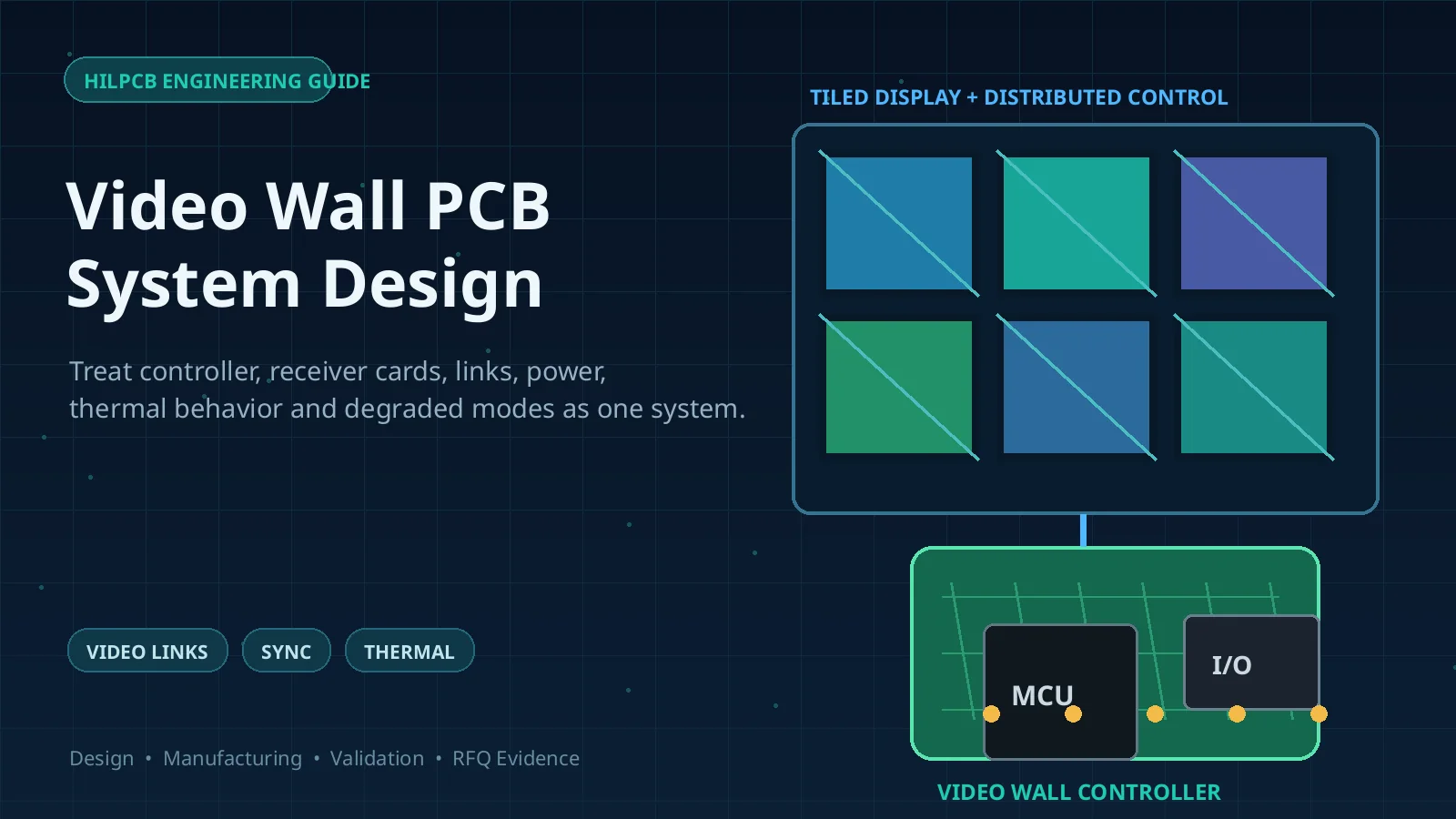
A video wall PCB is one of several circuit-board types that distribute, process, drive, power, or monitor image data in a tiled display system. A retail video wall is not controlled by one universal “display PCB”: it may include a media player, scaler, sending and receiving cards, cabinet HUB boards, LED driver modules, power-distribution boards, sensors, and network-management hardware.
Reliable design begins by freezing the display architecture and site requirements before choosing stackup, copper weight, laminate, connector, or cooling method. This guide links retail outcomes—readable content, color consistency, camera compatibility, uptime, serviceability, and operating cost—to the board-level evidence that can actually support them.
Key Takeaways
- Direct-view LED, tiled LCD, and projection walls have different electronics, optical behavior, maintenance models, and PCB risks. Smart or privacy glass is a separate product category.
- Pixel pitch should be selected from viewing distance and content needs; interface bandwidth should be calculated from resolution, frame rate, color depth, encoding, blanking, and redundancy—not from the word “4K” or “8K” alone.
- High-Tg laminate is not automatically thermally conductive, low-loss material is not automatically required, and thicker copper does not by itself solve LED temperature or voltage-drop problems.
- LED color and brightness consistency depend on binning, calibration, current regulation, PWM/scan timing, temperature, aging, optics, and controller settings as well as PCB manufacturing.
- Qualification should cover worst-case content, ambient light, wall-cavity temperature, airflow, camera shutter behavior, power faults, network loss, module replacement, and recovery—not only a bench image test.
- The best RFQ separates system-owner requirements from PCB fabrication, PCBA assembly, firmware, calibration, installation, and site acceptance responsibilities.
Contents
- What Boards Make Up a Retail Video Wall?
- Which Video Wall Technology Fits the Site?
- What Requirements Must Be Frozen Before PCB Design?
- How Should Video Bandwidth and Signal Integrity Be Designed?
- How Should Power Integrity Be Verified?
- How Should LED Heat and Color Uniformity Be Controlled?
- How Do You Design for Retail Uptime and Service?
- How Do You Diagnose Video Wall Failures?
- What Should the Verification Plan Include?
- What Should Be Included in a Video Wall PCB RFQ?
What Boards Make Up a Retail Video Wall?
System partitioning determines which PCB sees high-speed serial links, high-current LED loads, noisy switching converters, precision clocks, network traffic, or environmental exposure. Treating every board as an “LED wall PCB” hides these different constraints.
| Electronic layer | Primary function | Typical PCB risks | Evidence needed at release |
|---|---|---|---|
| Media player or edge computer | Decode content, run CMS client, schedule playback, handle local analytics | Memory and processor power, high-speed storage/display interfaces, thermal throttling, software security | Interface and thermal budgets, software image, watchdog/recovery test, cybersecurity ownership |
| Scaler or video processor | Crop, scale, synchronize, map, and sometimes color-process sources | Clocking, memory bandwidth, high-speed channel loss, reset and firmware behavior | Supported formats, latency/synchronization limits, channel simulation or compliance evidence, recovery test |
| Sending/transmitter card | Packetize or distribute mapped pixel data to cabinets | Multiport SI, connector/cable boundary, clock distribution, redundancy path | Port map, bandwidth per link, cable/connector limits, failover behavior, BER or protocol test |
| Receiving card | Recover data and generate cabinet/module control signals | Fanout, connector density, power sequencing, timing skew, firmware compatibility | Module map, output loading, timing/refresh settings, firmware and calibration revision |
| HUB or distribution board | Connect receiver, modules, power, sensors, and service interfaces | Connector current, ground return, hot-plug transients, cable errors, service damage | Current per contact, pin map, mating-cycle requirement, protection and continuity tests |
| LED module PCB | Hold LEDs, row/column drivers, decoupling, scan routing, and thermal paths | Current uniformity, switching noise, fine-pitch assembly, warpage, LED damage, local heating | LED/driver BOM control, scan scheme, current limits, photometric calibration input, thermal map |
| Power-distribution or PSU interface board | Distribute and protect DC rails across cabinets/modules | IR drop, connector heating, fault current, fuse/protection coordination, ground offset | Load cases, voltage-drop map, temperature rise, protection and fault-injection results |
| Monitoring and sensor board | Measure temperature, voltage, fan, door, smoke or ambient-light states as designed | Sensor placement, calibration, noisy ground, network attack surface | Sensor tolerances, alarm limits, calibration, event log and remote-monitoring test |
This architecture also clarifies procurement. A PCB supplier can fabricate and assemble released boards; the system owner still controls optical performance, content pipeline, controller firmware, calibration database, mechanical installation, electrical safety, network security, and final site acceptance unless those scopes are explicitly contracted.
Which Video Wall Technology Fits the Site?
Retail buyers should choose the display technology before optimizing the boards behind it.
| Display type | Strong fit | Main tradeoffs affecting electronics |
|---|---|---|
| Direct-view LED | Large seamless walls, unusual aspect ratios, high-impact brand areas, indoor or outdoor variants | Pixel pitch, viewing distance, module/cabinet service, brightness, scan/PWM behavior, calibration, power and heat |
| Tiled LCD | Menu boards, monitoring, and conventional rectangular layouts where narrow bezels are acceptable | Bezel visibility, panel matching, scaler and daisy-chain behavior, backlight aging, panel replacement availability |
| Projection or rear projection | Large images where throw path, optical engine, and controlled ambient conditions are practical | Optical alignment, light source, screen, ambient light, maintenance access; PCB design is centered in the projector/controller, not a tiled LED module |
Smart glass changes transmission or opacity and may be combined with media systems, but it is not a substitute name for a video wall PCB. It has different drive voltage, safety, optical, and installation requirements and should be specified as its own subsystem.
Direct-view LED product families span wide pixel-pitch ranges because the right pitch depends on viewing distance and image-detail expectations. A smaller pitch can improve close-view detail, but it also changes LED count, driver density, power distribution, thermal behavior, assembly yield, cost, and service strategy. Do not select pitch from resolution alone.
What Requirements Must Be Frozen Before PCB Design?
The engineering input should describe the actual store, content, and service model. Without it, “high-speed,” “high brightness,” and “24/7” are not testable requirements.
Optical and content requirements
- Physical wall dimensions, aspect ratio, native pixel map, minimum viewing distance, and expected content detail
- Indoor, window-facing, semi-outdoor, or outdoor location; ambient-light range; target luminance and contrast method
- Frame rates, color depth, chroma format, HDR or SDR workflow, scaling, rotation, and multi-source layout
- Camera exposure, shutter, frame-rate, or broadcast requirements if customers create social content or the wall appears on video
- Brightness-uniformity, color-uniformity, calibration, gray-scale, refresh, and replacement-module matching criteria
Site and operational requirements
- Supply voltage, branch-circuit limits, grounding, surge environment, emergency shutdown, and local code responsibility
- Ambient and wall-cavity temperatures, ventilation, dust, humidity, water exposure, altitude, sunlight, and cleaning agents
- Hours of operation, permitted degradation, maintenance window, front/rear service access, lifting and module-removal constraints
- Required redundancy for source, controller, data path, PSU, or network; acceptable behavior during failover
- CMS, network segmentation, remote monitoring, log retention, access control, privacy, and software-update ownership
Manufacturing and lifecycle requirements
- Prototype, pilot, and production volumes; expected installed lifetime; regional rollout; spares and last-time-buy policy
- Field-replaceable unit boundary, connector cycles, module serialization, calibration-data handling, and repair limits
- Applicable safety, EMC, environmental, flammability, energy, ingress, and market requirements by installation region
These inputs create acceptance limits for the PCB instead of forcing the PCB team to guess the system.
How Should Video Bandwidth and Signal Integrity Be Designed?
Start with the active pixel payload:
active payload = horizontal pixels × vertical pixels × frames per second × transmitted bits per pixel
That result is only a lower-bound planning value. The physical interface may add blanking, packet overhead, line encoding, forward-error correction, transport framing, or redundant data. Chroma subsampling or compression may reduce payload, while multiple mapped outputs redistribute it across links. The released calculation should identify every assumption and the required margin at each board, connector, and cable boundary.
The phrase “8K video wall” does not prove that every module PCB carries an 8K electrical interface. A central processor may receive the source and distribute smaller mapped regions over many links. Conversely, a modest panel may use a high-rate internal memory or serial interface. Partition the channel before selecting a laminate.
For each high-speed path on a high-speed PCB:
- Define source, sink, data rate, edge behavior, protocol, lane count, reference impedance, loss budget, and compliance method.
- Co-design stackup, trace geometry, reference planes, connector launch, via fields, layer changes, AC coupling, ESD protection, and return path.
- Limit stubs and discontinuities; use backdrilling or other structures only where the modeled channel and fabricator capabilities justify them.
- Model the PCB, connector, cable, and receiver boundary consistently; document S-parameter ports and de-embedding assumptions.
- Verify with the protocol's required test, eye/BER analysis, TDR/VNA correlation, or an agreed product-level method.
Do not select “Rogers/Teflon” from resolution labels. Standard or improved FR-4 families can be suitable when the channel is short and the loss budget permits; lower-loss material becomes justified when analysis shows that dielectric and conductor loss consume margin. High-Tg describes glass-transition behavior, not low loss or high thermal conductivity.
How Should Power Integrity Be Verified?
Video wall loads are spatially distributed and content-dependent. For a direct-view LED wall, full-white or another defined stress pattern may create a different current profile from typical content, while controller current limiting can change the peak. The test specification must define brightness, pattern, calibration state, refresh/scan settings, input voltage, ambient, and warm-up time.
Build a power tree from the site feed to the furthest LED or IC load. At every boundary, record nominal voltage, tolerance, current range, connector/contact rating, cable resistance, copper path, conversion efficiency, protection, and allowable temperature rise. DC simulation should include connector and cable drops, not only PCB copper.
On a multilayer PCB, solid planes, pours, stitching, local bulk capacitance, and high-frequency decoupling should be designed as a PDN across frequency. Closely spaced planes can contribute capacitance, but they are not a replacement for a complete decoupling network. Verify rail ripple and transients at the load during row switching, brightness steps, startup, failover, and communication events.
Thicker copper can reduce resistance in some paths, but it also affects etching, spacing, pad geometry, plane balance, weight, cost, and assembly. A heavy-copper PCB is appropriate only when current, temperature-rise, fabrication, and layout analyses support it. Power connectors, fuses, cables, and contacts may remain the limiting elements.
Power-release evidence
- Worst-case and representative content current at system, cabinet, and module levels
- Minimum input-voltage operation and far-end voltage-drop map
- Rail ripple, transient, startup, shutdown, brownout, recovery, and fault-injection results
- Connector/contact, fuse, converter, cable, and copper temperature-rise measurements
- Protection selectivity and behavior for short, open load, reversed connection, failed fan, or lost data as applicable
- Energy-use assumptions separated from marketing content averages
How Should LED Heat and Color Uniformity Be Controlled?
LED junction temperature, driver temperature, converter losses, ambient conditions, optical construction, module spacing, enclosure conduction, and airflow form one thermal system. A PCB thermal via can help only if it connects the heat source to an effective spreading and removal path.
Use component loss estimates and a system thermal model to identify hotspots, then correlate at worst-case input, content pattern, brightness, ambient, orientation, and airflow. Measure the wall cavity as well as exposed room air. A bench module with unrestricted convection does not represent a densely tiled installation.
High-Tg laminate may retain mechanical properties better at elevated temperature, but it is not automatically high-conductivity material. A metal-core PCB can offer a useful conduction path for some LED module architectures, yet it may not suit multilayer high-density routing or isolation requirements. Thermally conductive dielectric, copper spreading, vias, heat spreaders, chassis interfaces, fans, and power derating must be evaluated together.
Color and brightness uniformity also require system controls:
- Locked LED manufacturer, package, binning strategy, and approved substitution rules
- Driver-current accuracy, resistor tolerance, scan ratio, PWM bit depth, refresh behavior, and low-gray performance
- Optical masks, coatings, module flatness, cabinet alignment, viewing angle, and reflection control
- Factory calibration method, measurement instrument, calibration-map version, storage location, and field replacement process
- Temperature compensation, aging compensation, brightness limits, and post-service recalibration where implemented
Do not publish universal temperature reductions, lifetime extensions, maintenance savings, or uptime percentages without product-specific test and field data. PCB improvements can reduce identified thermal stress, but display lifetime remains a system claim.
How Do You Design for Retail Uptime and Service?
Retail downtime is not solved by specifying “high reliability” on the PCB drawing. Availability depends on fault containment, monitoring, spares, access, diagnosis, replacement time, configuration control, and the behavior customers see during a fault.
Define field-replaceable units before layout. Front-service modules reduce rear-access needs but impose connector, handle, alignment, tool, and hot-swap constraints. A receiving card or PSU should be replaceable without corrupting adjacent calibration data or creating an unsafe live-work procedure. Keyed and polarized connectors, unambiguous labels, strain relief, touch protection, and board support reduce service-induced failures.
Redundancy must have a failure model. Dual links are not useful if they share one connector, regulator, clock, firmware defect, or network switch that can fail both paths. Test failover with cable removal, controller reset, PSU loss, corrupted content, network outage, thermal alarm, and invalid module configuration as applicable. Record whether the wall freezes the last frame, blacks out, degrades locally, switches sources, or raises an alarm.
Remote monitoring should expose actionable states such as cabinet/module temperature, input voltage, PSU/fan status, data-link error, receiving-card status, door state, and firmware/calibration revision where supported. Networked signage also needs authenticated updates, least-privilege access, log protection, vulnerability response, and privacy controls for any cameras or analytics. These are system and software responsibilities, not properties proven by a bare PCB inspection.
How Do You Diagnose Video Wall Failures?
The following matrix prevents premature blame. A visible symptom may arise from content, software, network, controller, cable, PCB, component, optics, mechanics, power, temperature, or calibration.
| Site symptom | Possible board/system domains | First useful evidence | Do not conclude from symptom alone |
|---|---|---|---|
| One dead module or row | LED/driver, HUB connector, receiving-card output, local rail, cable, configuration | Swap boundary, rail/current measurement, connector continuity, mapped test pattern, error log | “All LEDs are defective” or “the receiver card failed” |
| Intermittent snow, sparkles, or link loss | Source format, channel loss, connector/cable, clock, EMI, receiver margin, power transient | Link counters, known-good cable/port swap, eye/BER or protocol test, rail capture | “Needs lower-loss laminate” |
| Tearing or unsynchronized areas | Controller mapping, genlock/frame sync, firmware, data path, mixed revisions | Source/frame configuration, controller logs, revision map, synchronized test content | “PCB impedance is wrong” |
| Uneven brightness across wall | Calibration map, LED bins/aging, temperature, voltage drop, optics, driver current | Photometric grid, module temperature, far-end rail, calibration and BOM revisions | “Add thicker copper” |
| Color shift after warm-up | LED temperature, calibration/compensation, driver drift, optics, ambient light | Warm-up trend, temperature map, calibrated color measurement, rail/current stability | “LEDs are low quality” |
| Camera bands or scan lines | PWM/refresh/scan timing, camera shutter/frame rate, content cadence | Camera settings, controller refresh/PWM configuration, high-speed optical measurement | “The human-visible image is defective” |
| Connector or cable heating | Contact resistance, current sharing, mating, crimp, overload, contamination, airflow | Temperature rise, millivolt drop, current per contact, connector inspection | “PCB copper is undersized” |
| Thermal shutdown or dimming | Cavity ambient, blocked airflow, fan/PSU, content load, sensor placement, firmware limits | Event log, thermal/current map, airflow state, stress pattern and ambient | “MCPCB will fix the whole wall” |
| Replaced module does not match | LED lot, calibration data, firmware, optics, cabinet alignment | Serial/BOM/calibration map, instrumented recalibration, mechanical alignment | “Replacement PCB passed, so it must match visually” |
Convert recurring symptoms into a fault-insertion test. If a lost receiver link previously blacked out multiple cabinets, reproduce it under controlled conditions and verify the revised containment and alarm behavior.
What Should the Verification Plan Include?
PCB and PCBA evidence
- Stackup, impedance requirements, coupons, material identity, drill/backdrill data, copper and finish records
- AOI, X-ray, electrical test, programming, boundary/functional test, and first-article evidence selected by package and risk
- Rail resistance, current capacity, connector derating, temperature rise, and protection validation
- Firmware, FPGA image, calibration map, test program, fixture, instrument, and board revisions linked to serial or lot
Display and system evidence
- Supported source formats, scaling/mapping, latency, synchronization, failover, boot, brownout, and recovery
- Brightness, contrast method, color, gray scale, uniformity, refresh/PWM, camera behavior, and replacement-module matching
- Worst-case thermal and power tests at defined ambient, airflow, brightness, content, and wall configuration
- Network loss, remote alarm, access control, software update, rollback, log, and cybersecurity-response checks
- Installation inspection for structure, grounding, cooling, clearances, cable routing, service access, and site power
Reliability and scope boundary
Environmental and lifetime testing must reflect the product: thermal cycling, damp heat, vibration, drop/impact, dust/water exposure, corrosion, UV, cleaning chemicals, connector cycling, or burn-in may apply. The system owner should derive the stress profile and sample plan from use conditions and risk; passing one generic “aging test” is not a universal reliability claim.
What Drives Video Wall Cost?
Pixel pitch and wall area drive LED count, but total cost also includes controller ports, receiving cards, cabinets, PSU capacity, cooling, calibration, structure, installation, service access, spares, content systems, test fixtures, and field support. Lower-loss laminate or heavier copper should appear only where engineering evidence justifies the recurring cost.
Compare architectures using total lifecycle assumptions:
- Initial display, electronics, structure, installation, commissioning, and content integration
- Energy and cooling at defined operating profiles
- Calibration labor, planned cleaning, module/PSU/fan replacement, access equipment, and service response
- Spare-module lot strategy and risk of visible mismatch years later
- Controller, firmware, CMS, and network-support lifecycle
- Cost and customer impact of a local degraded area versus a wall-wide outage
The RFQ should separate non-recurring engineering—SI analysis, fixtures, calibration setup, tooling, software—from unit and field costs.
What Should Be Included in a Video Wall PCB RFQ?
System and optical inputs
- Display technology, wall dimensions, native resolution, pixel pitch, cabinet/module map, minimum viewing distance, and service direction
- Source formats, frame rate, color depth/chroma, HDR/SDR, latency/sync, camera, brightness, uniformity, and calibration requirements
- Indoor/outdoor exposure, ambient and cavity temperature, humidity, dust/water, sunlight, altitude, ventilation, duty cycle, and cleaning
Electrical and PCB inputs
- Architecture block diagram and responsibility boundary for player, controller, sending/receiving cards, HUB, modules, PSUs, sensors, network, and firmware
- Schematics, BOM with approved alternates, fabrication/assembly data, stackup, impedance table, mechanical drawings, connector/cable definitions, and netlist
- Link budgets, simulations/models, power tree, current/load cases, rail limits, protection, grounding, EMC, thermal model, and test points
Production, test, and service inputs
- Prototype/pilot/production quantities, panelization, traceability, firmware/programming, calibration, inspection class, functional limits, and retained records
- Field-replaceable units, module serialization, calibration-data transfer, spares, repair limits, connector cycles, and service tools
- Reliability, safety, EMC, ingress, flammability, environmental, energy, network-security, and regional installation requirements
- Change-notification and requalification triggers for LED/driver/connector/laminate/stackup/PSU/controller/firmware/calibration/process substitutions
HILPCB can review the released board package for fabrication, turnkey PCB assembly, high-speed interconnects, power distribution, component sourcing, and testability. The quote should state which simulations, fixtures, calibration, firmware, optical tests, environmental tests, and system certifications are included or remain customer-owned.
Reference Standards and Specifications
Confirm current revisions and regional applicability with the system integrator and authority having jurisdiction.
- AVIXA V202.01 — AVIXA
- IEC 62368-1 — International Electrotechnical Commission
- CISPR 32 — International Special Committee on Radio Interference
- CISPR 35 — International Special Committee on Radio Interference
- IEC 60529 — International Electrotechnical Commission
- IPC-2221 — IPC
- IPC-6012 — IPC
- IPC-A-610 — IPC
- Applicable source-interface and controller manufacturer specifications
- Applicable building, electrical, structural, fire, accessibility, privacy, and outdoor-sign requirements
Common Questions
Does an 8K video wall require a low-loss RF laminate?
Not automatically. The source resolution does not reveal the data rate or length on each PCB channel. Partition the system, calculate interface bandwidth, build the loss budget, and model the actual trace, via, connector, and cable path before selecting material.
Is a smaller LED pixel pitch always better for retail?
No. Smaller pitch can improve close-view detail but increases pixel and driver density, cost, power/thermal complexity, and service sensitivity. Choose pitch from minimum viewing distance, wall size, content detail, brightness, camera use, installation, and lifecycle cost.
Does a high-Tg PCB dissipate LED heat better?
Not by definition. Tg describes a laminate transition property, not its through-plane thermal conductivity. Thermal performance depends on component losses, copper, vias, dielectric, spreaders, chassis interfaces, airflow, ambient conditions, and the complete heat-removal path.
What causes brightness variation across an LED wall?
Possible causes include LED binning and aging, calibration data, driver-current tolerance, PWM/scan settings, voltage drop, temperature, optical masks, cabinet alignment, and replaced module lots. Use photometric, electrical, thermal, BOM, and calibration evidence together.
What should be tested before shipping a retail video wall PCB?
Test the risks assigned to that board: fabrication continuity and impedance, assembly defects, programming, rails and protection, high-speed links, drivers/outputs, sensors, thermal load, and functional interfaces. Optical calibration, full-wall failover, installation, EMC, safety, and site acceptance remain separate unless explicitly included.
Conclusion
A reliable retail video wall begins with system partitioning, measurable site requirements, and clear ownership. PCB engineering then supports the result through validated high-speed channels, low-impedance power distribution, controlled LED-driver timing, credible thermal paths, protected interfaces, test access, and revision-linked manufacturing evidence.
Do not buy material labels or unsupported uptime claims. Release the pixel map, bandwidth assumptions, load cases, thermal environment, calibration plan, service model, fault behavior, and acceptance tests with the PCB data. HILPCB can then quote the board and assembly work against defined evidence while the display integrator retains control of optical performance, installation, content, software, cybersecurity, and final site acceptance.