
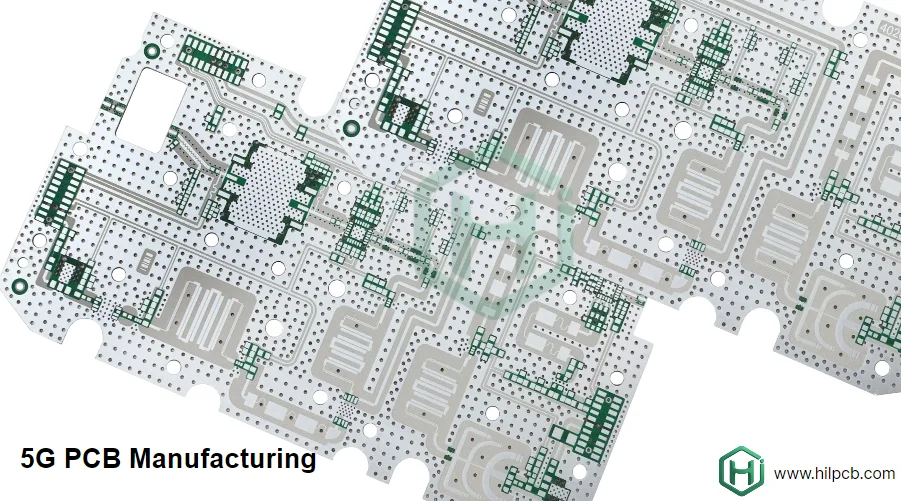
- 5G PCB technology should be reviewed as an RF-system implementation problem across defined frequency ranges, not as a generic "faster telecom PCB" label.
- The first checks are whether the design sits in FR1 or FR2, what insertion-loss budget the path allows, whether the stackup supports stable impedance, how shielding and grounding are partitioned, and how the build will actually be validated.
- Most project failures come from vague material selection, mixing digital and RF constraints without a clear floorplan, ignoring transition structures, or claiming mmWave readiness before measurement access exists.
- The right board choice depends less on a marketing term like "5G-ready" and more on path length, laminate stability, package transitions, thermal load, and production repeatability.
- Prototype success usually depends on freezing stackup, launch geometry, shielding approach, and RF test strategy before the first build.
5G PCB technology refers to the material, stackup, routing, shielding, and manufacturing decisions used to support 5G radio hardware across sub-6 GHz and, where relevant, FR2/mmWave ranges. The practical engineering question is whether the board can preserve signal quality, phase consistency, thermal stability, and manufacturability at the actual operating band.
Contents
- What to review first in 5G PCB technology
- Key design and validation rule table
- Early engineering trade-off table
- How FR1 and FR2 change material and stackup decisions
- How transitions, shielding, and thermal path affect real RF performance
- What prototype teams should freeze before release
- FAQ
- Next steps
- References
- Author and review
What to review first in 5G PCB technology
According to 3GPP, 5G NR is split into FR1 and FR2 ranges, and that distinction matters because the board problem changes materially with frequency. A board that works well in lower-frequency radio hardware may still be inappropriate for higher-loss or more phase-sensitive structures.The first review points are usually:
- whether the product operates in FR1, FR2, or a mixed architecture with different RF constraints
- whether the critical paths need specialty laminate, hybrid stackup, or simply stronger discipline on geometry and return paths
- whether RF launches, vias, connectors, and package transitions dominate loss or mismatch more than the trace segment itself
- whether power, digital control, synchronization, and RF zoning are partitioned early enough to avoid late shielding problems
- whether the validation plan includes coupon, VNA, TDR, and assembled-path measurement instead of only layout simulation
These points map directly onto a DFM/DFT/DFA review for 5G boards.
For radio and phased-array hardware, it is usually worth aligning high-frequency PCB, Rogers PCB, and multilayer PCB assumptions before release.
Key design and validation rule table
| Rule / parameter | What to check first | Why it matters | How to verify | If ignored | | --- | --- | --- | --- | --- | | FR1 vs FR2 context | Define the real operating range and architecture first | The board strategy changes with loss, phase sensitivity, and packaging | System review and RF path map | Over- or under-designed stackup | | Material fit | Choose laminate by loss stability and processing fit, not headline brand alone | Wrong material assumptions distort insertion loss and impedance repeatability | Datasheet review and stackup review | Weak RF margin and avoidable cost | | Transition control | Review launches, vias, connectors, and module boundaries early | Discontinuities often hurt performance more than straight traces | Launch review and field-solver correlation | Mismatch, reflections, unstable channels | | RF/digital partitioning | Separate RF, bias, control, and power return structure intentionally | Dense radio boards fail when domains share uncontrolled paths | Floorplan review and grounding review | EMI, coupling, poor repeatability | | Shielding and mechanical path | Define shields, covers, and thermal attachments as part of the design | Mechanical details change RF behavior in the real product | Assembly review and pilot build inspection | Good simulation, weak real hardware | | Measurement access | Decide how critical paths will be tested after fabrication and assembly | A 5G claim is weak if the RF path cannot be measured realistically | Test plan and coupon strategy | Debug delays and unclear acceptance |Early engineering trade-off table
| Design choice | Usually stronger for | Main trade-off | What to confirm early | | --- | --- | --- | --- | | Hybrid RF + FR-4 stackup | Balancing cost and practical integration in mixed systems | Stronger lamination and partition control needed | Which layers truly need low-loss material | | Full low-loss stackup | Higher-band and more phase-sensitive paths | Higher cost and process burden | Whether the whole board benefits materially | | Denser HDI support routing | Compact control and support circuitry near radio modules | More process complexity and inspection burden | Package pitch and via strategy | | Heavier shielding | Better isolation in crowded radio sections | Harder thermal and service access | Mechanical envelope and debug route | | Integrated radio module board | Shorter paths and tighter packaging | Less forgiving thermal and assembly window | Heat extraction and test access | | Split RF and digital sections | Cleaner electrical partitioning | More connectors or interconnect complexity | Signal boundary definition |How FR1 and FR2 change material and stackup decisions
The main mistake in 5G board discussions is acting as if every 5G PCB needs the same material set. It does not. The board should be chosen around the actual path sensitivity and loss budget.Three questions usually matter most.
1. Is the board really solving an FR1 problem or an FR2 problem?
3GPP defines FR1 and FR2 as separate operating ranges, and the design burden rises sharply when loss, launch quality, and phase stability become more sensitive. Some projects need full mmWave discipline. Others mainly need better RF partitioning and material control in sub-6 GHz hardware.
2. Does the critical path justify specialty laminate?
Rogers and other RF material suppliers show that low-loss laminates help preserve electrical consistency, but they do not remove the need for careful transitions, grounding, and manufacturing control. Material selection should follow path need, not marketing inertia.
3. Is the stackup helping or hiding the real problem?
Hybrid builds often work well when only part of the board carries the most sensitive RF energy. But the stackup only helps if launch structures, copper distribution, and lamination behavior are planned coherently.
How transitions, shielding, and thermal path affect real RF performance
Boards sold as "5G technology" often fail in the details around the trace. Real RF behavior depends on how packages, vias, shields, connectors, and thermal interfaces change the path after manufacturing and assembly.The main engineering checks are:
- whether launch transitions into modules, antennas, or connectors are modeled and inspectable
- whether shields improve isolation without blocking service or trapping heat
- whether nearby PA, clock, and power sections inject noise or thermal drift into sensitive RF structures
- whether the validation route includes both fabricated coupons and assembled-path checks
If the product combines dense RF, digital support, and module assembly, HDI PCB, SMT assembly, and PCB prototype planning usually needs to happen together.
What prototype teams should freeze before release
The first 5G hardware build should prove the real path, not just the concept drawing. Before release, the team should know which paths are critical, how they will be built, and how they will be measured.A practical release checklist usually includes:
- Operating band and critical paths frozen
Confirm whether the board problem is FR1, FR2, or a mixed architecture. - Material and stackup approved
Lock the laminate family, copper balance, and reference structure before detailed tuning starts. - Launch and transition review completed
Approve vias, connectors, package escapes, and RF boundary structures as one system. - Shield and thermal approach documented
Define how mechanical hardware changes RF and heat behavior after assembly. - Measurement plan approved
Freeze coupon, TDR, VNA, and assembled-path checks before pilot build. - Revision and BOM review completed
Use a BOM viewer and Gerber viewer review to catch substitutions or geometry changes before release.
If the launch geometry is still moving, quick-turn PCB support is usually more useful than forcing a production-style run.
FAQ
Does every 5G PCB need low-loss RF laminate?
No. It depends on the operating band, path length, insertion-loss budget, and how sensitive the hardware is to phase and mismatch.
What is the first thing to define in a 5G PCB project?
Usually the real frequency context, especially whether the board problem sits in FR1, FR2, or a mixed architecture.
Why do some 5G boards fail even with good material choices?
Because launch structures, grounding, shielding, and assembly details can dominate performance if they are not designed and validated together.
Is hybrid stackup a compromise or a good engineering choice?
It can be a very good engineering choice when only part of the board needs specialty RF material and the lamination strategy is controlled properly.
What should be frozen before the first prototype release?
Freeze the operating band assumptions, stackup, transitions, shielding plan, and RF validation route.
Next steps
If you are planning 5G radio, beamforming, or other communication equipment PCB hardware, the most useful next step is usually to review frequency range, stackup, launches, and measurement method together before prototype release.
HILPCB can support that process through:
- High-frequency PCB and Rogers PCB planning for low-loss RF paths
- Multilayer PCB and HDI PCB support for dense mixed-domain designs
- SMT assembly coordination for shielded radio module builds
- PCB prototype, quick-turn PCB, Gerber viewer, and PCB viewer for early validation
- Request a quote when your stackup, RF boundaries, and validation notes are ready