
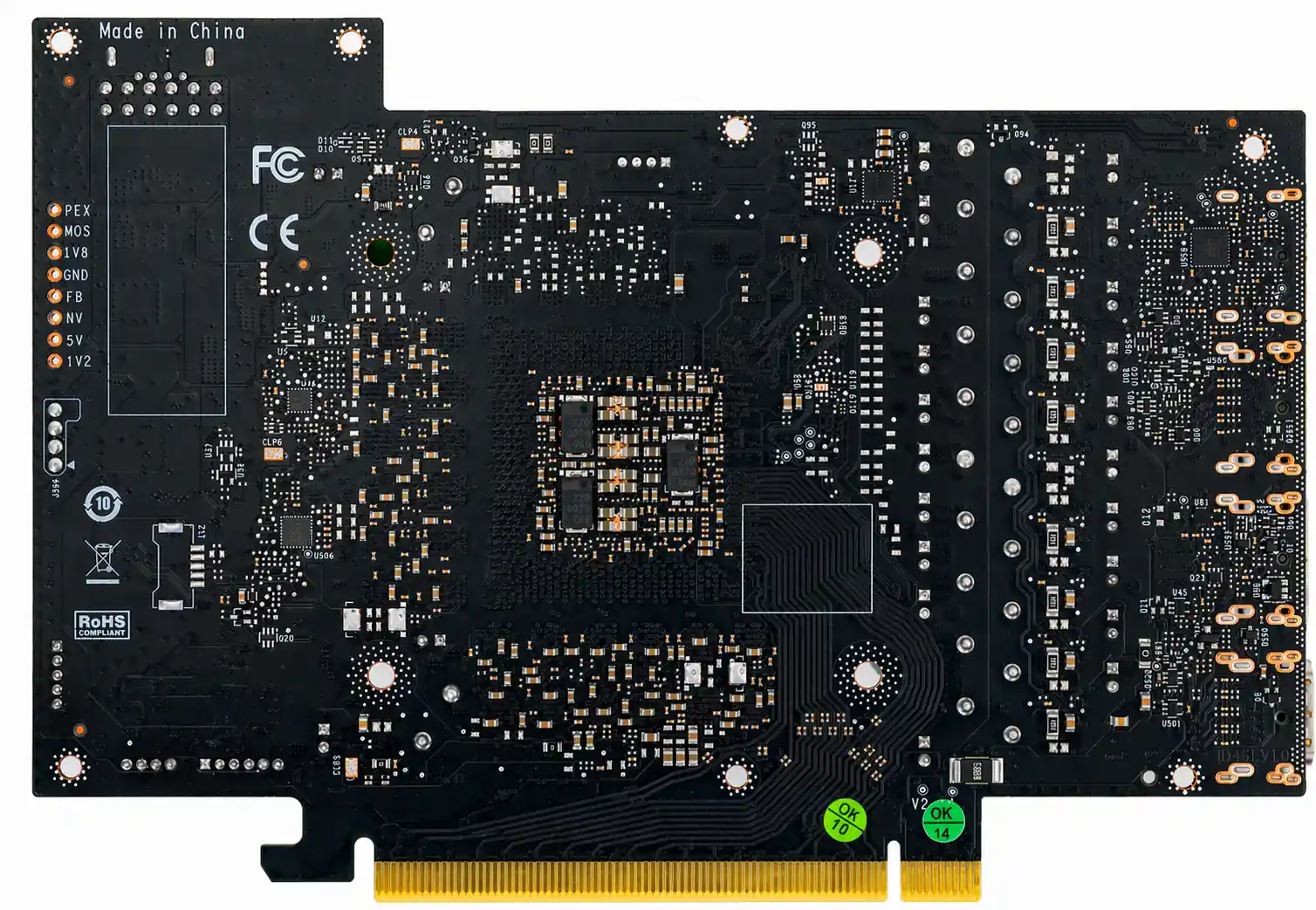
20 layer PCBs push interconnect density into the realm of advanced HDI, where traditional through-hole vias and simple blind/buried structures can no longer support the routing requirements of modern high-pin-count devices. At this layer count, designs increasingly adopt any-layer HDI—also known as ELIC (Every Layer Interconnect)—where microvias on every layer can connect to any adjacent layer, forming free-form vertical interconnection across the entire 20 layer stack through stacked, copper-filled microvia structures.
Any-layer HDI at 20 layers is not simply "more of the same" HDI used at lower layer counts. It requires a fundamentally different manufacturing approach: instead of building up around a pre-fabricated multilayer core, the board is constructed layer by layer through 10 or more sequential lamination, drilling, and plating cycles. Each cycle adds one layer of dielectric and copper, with microvias connecting to the layer below. The result is a board where any point on any layer can connect to any point on any adjacent layer—providing routing freedom that no other via technology can match.
This guide covers the manufacturing process, material requirements, design rules, and reliability qualification for 20 layer any-layer HDI PCBs—the technology that enables the most interconnect-dense designs in commercial electronics.
Procurement teams and NPI managers from leading technology companies in California, Massachusetts, and Western Europe select HILPCB for any-layer HDI builds because of our proven stacked microvia reliability, competitive pricing on advanced constructions, and the manufacturing discipline needed to maintain yield across 10+ sequential lamination cycles.
HILPCB Manufacturing Capability: We fabricate 20 layer PCBs with any-layer HDI, copper-filled stacked microvias spanning up to 6 layers, trace/space down to 2.5/2.5mil, and IST-verified microvia reliability exceeding 200 thermal cycles—from NPI prototypes through production volumes.
In This Guide
- The Density Challenge That Drives 20 Layer HDI
- Any-Layer HDI vs. Conventional HDI: What Changes at 20 Layers
- The Sequential Build Process: Layer by Layer
- Copper Filling: The Critical Technology
- Material Systems for 20 Layer ELIC
- Design Rules for Any-Layer HDI
- Reliability Testing: IST and Failure Mode Analysis
- 20 Layer Boards with High-Frequency and Rigid-Flex Options
- Advanced HDI Manufacturing at HILPCB
The Density Challenge That Drives 20 Layer HDI
Three concurrent technology trends drive the need for 20 layer any-layer HDI:Ultra-fine-pitch BGA devices. Modern application processors, networking ASICs, and high-end FPGAs use BGA packages with 0.4-0.5mm pitch and ball counts exceeding 2000. Escaping all signals requires microvia connections on nearly every layer beneath the device footprint. Conventional HDI (1+N+1 or 2+N+2) limits blind vias to the outer 1-2 layers per side, constraining escape capacity.
Multi-die integration. System-in-Package (SiP) and chiplet architectures place multiple high-pin-count devices in close proximity, creating routing congestion between devices that cannot be resolved with through-hole vias blocking all layers.
Board miniaturization. For networking line cards, avionics modules, and medical instruments where board area is fixed, 20 layer HDI enables more functionality by stacking routing capacity vertically rather than spreading it horizontally.
Any-Layer HDI vs. Conventional HDI: What Changes at 20 Layers
| Feature | Conventional HDI (2+N+2) | Any-Layer HDI (ELIC) | | :--- | :--- | :--- | | Microvia layers | Outer 2 per side only | Every layer | | Core structure | Central mechanically-drilled core | No core (or thin central core) | | Via spanning | Microvia = 1-2 layers; core vias = full depth | Microvia = 1 layer; stacked = any depth | | Layer connectivity | Limited to buildup-to-core transitions | Any layer to any adjacent layer | | BGA escape capacity | Limited by buildup layer count | Scales with total layer count | | Manufacturing complexity | 2-3 lamination cycles | 10+ lamination cycles |Practical Compromise: Hybrid ELIC/Core
Full 20 layer ELIC (18 lamination cycles) is extremely expensive. A practical compromise uses a conventional multilayer core with ELIC buildup—for example, 5+10+5: 10-layer core with through-hole and buried vias, plus 5 ELIC buildup layers per side. This reduces lamination cycles to 5 per side while providing any-layer connectivity across the outer layers where fine-pitch BGA connections occur.
The Sequential Build Process: Layer by Layer
For a 5-high stacked microvia (L1 through L5):Substrate preparation: The core or previous buildup has completed L5 copper patterning with landing pads defined.
Dielectric application: Resin-coated copper (RCC) or prepreg is laminated onto L5, forming the L4-L5 dielectric (typically 40-80μm for RCC).
Laser drilling: UV or CO2 laser drills microvias from L4 surface to L5 landing pads. Diameter: 60-100μm top, 40-60μm bottom (tapered).
Desmear and seed: Plasma desmear cleans the via bottom. Electroless copper deposits a conductive seed layer on via walls and bottom.
Copper filling: Electrolytic copper fills the microvia completely using specially formulated chemistry with organic additives (suppressors, accelerators, levelers) that achieve void-free bottom-up fill.
Planarization: Mechanical polishing creates a flat surface (±5μm) for the next microvia landing pad.
Patterning: Photolithographic imaging and etching define the L4 copper pattern.
Repeat: Steps 2-7 for each subsequent layer (L3, L2, L1).
Critical Process Parameters
- Laser drilling precision: Each microvia must center on the filled pad below within ±15-25μm. Pattern recognition systems align to fiducials on the just-plated layer.
- Copper fill quality: Any void or seam becomes a crack initiation site during thermal cycling. Fill must be 100% void-free with dimple ≤5μm.
- Planarization: Surface flatness within ±5μm across the panel—over-polishing exposes dielectric; under-polishing causes laser drilling depth errors on the next layer.
 This is a 20-layer Any-Layer HDI PCB
Copper Filling: The Critical Technology
Copper filling is the single most critical process in stacked microvia manufacturing. The fill must be completely void-free, flat-surfaced, and metallurgically sound to survive the thermal stress of subsequent lamination cycles and field operation.Fill Process Chemistry
The copper fill uses specially formulated plating chemistry where: accelerators concentrate at the via bottom (concave surface), increasing local plating rate; suppressors concentrate at the via top and field copper, slowing plating rate; and levelers smooth the surface as filling progresses. This differential produces bottom-up fill, closing the via completely without trapping voids.
Fill Quality Specifications
| Parameter | Specification |
|---|---|
| Fill completeness | 100% void-free on cross-section |
| Surface dimple (concavity) | ≤5μm |
| Surface protrusion (convexity) | ≤10μm |
| Copper grain structure | Columnar or equiaxed (no laminar voids) |
| Peel strength on filled surface | ≥6 lb/in |
Material Systems for 20 Layer ELIC
### Buildup Layer MaterialsResin-Coated Copper (RCC / ABF): Preferred for ELIC buildup. Provides the thinnest dielectric (40-80μm), contains no glass reinforcement (clean UV laser drilling), and produces smooth via walls. Dk typically 3.3-3.5, Df 0.005-0.010 at 1GHz.
Ultra-thin prepreg: For buildup layers requiring glass reinforcement, styles 1027 (28μm glass) or 1017 (15μm glass) can be laser-drilled. CO2 lasers handle up to ~3mil glass-reinforced dielectric; UV lasers handle up to ~2mil.
Core Material Requirements
Core materials must survive 10+ press cycles at 180-200°C. Materials with Tg ≥180°C and Td ≥340°C are mandatory. Isola 370HR, Panasonic Megtron 6, and ITEQ IT-988SE are proven core materials.
Copper Foil
Ultra-thin copper (9-12μm) enables fine-line etching at 2.5/2.5mil trace/space. Low-profile (LP) or very-low-profile (VLP) copper (Rz <3μm) reduces conductor loss for high-speed signals above 10Gbps.
Design Rules for Any-Layer HDI
| Parameter | Standard | Advanced | | :--- | :--- | :--- | | Microvia top diameter | 100μm | 75μm | | Microvia bottom diameter | 60μm | 40μm | | Capture/target pad | 250μm | 200μm | | Stacked height (max) | 5 layers | 7 layers | | Trace width (min) | 3mil (75μm) | 2.5mil (63μm) | | Trace space (min) | 3mil | 2.5mil | | Registration per layer | ±25μm | ±15μm |Stack Height Limits
Industry practice limits stacked microvias to 5-6 layers for standard reliability. Each additional layer increases cumulative thermal stress—the bottom microvia in a 5-high stack experiences 5 reflow cycles during buildup construction plus additional reflows during assembly. Stacks of 7+ require enhanced copper fill chemistry, optimized planarization, and additional reliability qualification (typically 300+ IST cycles instead of 200).
Impedance on Thin Dielectrics
ELIC buildup layers have thin dielectric (2-3mil), producing tightly coupled microstrip/stripline with narrow trace widths for 50Ω. On 2mil RCC (Dk 3.4), a 50Ω microstrip requires approximately 3.0mil trace width—at the edge of standard photolithographic capability.
For differential pairs at 100Ω on thin RCC dielectric, individual trace widths drop to approximately 2.0-2.5mil with 3-4mil spacing. Manufacturing these geometries consistently requires Laser Direct Imaging (LDI) rather than conventional photomask exposure, and modified etch chemistry for controlled undercut.
Registration Budget for Stacked Microvias
Registration is the most critical geometric control for any-layer HDI. Each buildup layer adds ±15-25μm of registration uncertainty. Over a 5-high stack, the cumulative misregistration can reach ±75-125μm:
| Stack Height | Cumulative Registration (worst case) | Min. Capture Pad Required |
|---|---|---|
| 2-high | ±30-50μm | 200μm |
| 3-high | ±45-75μm | 225μm |
| 4-high | ±60-100μm | 250μm |
| 5-high | ±75-125μm | 275μm |
| 6-high | ±90-150μm | 300μm |
Advanced global fiducial alignment systems achieve ±15μm per layer, reducing 5-high cumulative error to ±75μm and enabling the 200μm capture pads that fine-pitch BGA escape requires.
DFM Optimization for 20 Layer HDI
Via pad sizing strategy: Use graduated pad sizes—largest on L1 (surface), decreasing on inner layers. This maximizes routing density on inner layers where space is most constrained.
Copper balance per buildup layer: Maintain copper density within ±15% between L1 and L20 to minimize warpage. RCC buildup layers are especially sensitive because they lack glass reinforcement and depend on copper stress balancing for dimensional stability.
Panel utilization: Any-layer HDI has lower panel utilization than conventional boards—larger border areas for IST coupons and process monitoring. Plan for this when calculating unit cost.
Design for test: Include test point access on at least two outer layers. With 20 layers, ICT (in-circuit test) probe access becomes challenging—consider boundary scan JTAG for functional testing of buried connections.
The Cost Structure of 20 Layer Any-Layer HDI
Understanding the cost drivers helps engineers decide between full ELIC and hybrid approaches:
| Cost Element | ELIC (10+10) | Hybrid (5+10+5) | Standard 20L |
|---|---|---|---|
| Lamination cycles | 18 | 10 | 2-3 |
| Laser drill cycles | 18 | 10 | 0-2 |
| Copper fill cycles | 18 | 10 | 0 |
| Material cost | Highest (RCC) | Medium | Lowest (FR-4) |
| Registration difficulty | Extreme | High | Standard |
| Yield (typical) | 60-75% | 75-85% | 85-95% |
| Unit cost relative to standard | 5-8× | 3-5× | 1× |
The hybrid 5+10+5 approach offers the best price/performance ratio for most applications: any-layer connectivity where BGA escape demands it (outer layers), conventional through-hole economy where it doesn't (inner core).
Lead Time Considerations
Full ELIC 20 layer boards require 20-30 business days for prototype fabrication—each lamination cycle takes 1-2 days including setup, pressing, and cooling. Hybrid constructions (5+10+5) reduce lead time to 15-20 days because the inner core can be fabricated in parallel with outer layer preparation. Production volume lead times improve as process setup is amortized across panels.
Reliability Testing: IST and Failure Mode Analysis
### IST (Interconnect Stress Test)IST is the gold standard for HDI microvia reliability. A daisy-chain coupon connects all stacked microvias in series. The coupon is rapidly thermal cycled (room temperature to 150°C, ~200 cycles/hour) while continuously monitoring resistance. A resistance increase >10% indicates failure.
IPC requirements: stacked microvias must survive 200 IST cycles per IPC-2315. HILPCB qualifies production lots to 300+ cycles for additional margin.
Failure Modes
| Mode | Mechanism | Detection |
|---|---|---|
| Barrel crack | CTE mismatch stress | Cross-section, IST |
| Bottom separation | Incomplete fill or poor adhesion | Cross-section, continuity |
| Stack fracture | Cumulative stress across multi-layer stack | IST monitoring |
| Void expansion | Micro-voids expand during reflow | X-ray, cross-section |
Cross-Section Sampling
Production 20 layer HDI boards require higher sampling rates: first article has full cross-section set of all unique via configurations; production lots require one set per 50 panels.
20 Layer Boards with High-Frequency and Rigid-Flex Options
### High-Frequency 20 Layer ConstructionsFor networking line cards and data center switches carrying 56G-112G SerDes, 20 layer boards may use low-loss core materials (Megtron 6) with RCC buildup. VLP copper on high-speed signal layers reduces conductor loss at multi-GHz frequencies.
Rigid-Flex at 20 Layers
20 layer rigid-flex constructions serve ultra-compact aerospace and medical systems. The flex layers (typically 2-4) carry signals between rigid sections containing the full 20 layer HDI stack-up.
IC Substrate Bridge
HILPCB's IC substrate capability extends ELIC concepts into semiconductor-grade packaging with SAP fine-line processing (15-20μm trace/space).
Process Control Depth: What Separates Production-Grade ELIC from Prototyping
Copper Fill Bath Chemistry: The Hidden Variable
The electrolytic copper fill process uses a delicate balance of three organic additive families: accelerators (SPS—bis(3-sulfopropyl) disulfide), suppressors (PEG—polyethylene glycol), and levelers (JGB—Janus Green B or proprietary compounds). These additives are consumed during plating and degraded by chemical interaction—a bath that produces perfect fills on Day 1 will produce 5-10% voiding by Day 3 without intervention.
HILPCB runs CVS (Cyclic Voltammetric Stripping) analysis on fill bath chemistry every 8 hours during ELIC production. Accelerator concentration is maintained within ±5% of target, and suppressor/leveler ratios are adjusted based on real-time analysis rather than fixed schedules. This analytical rigor is what allows us to maintain zero-void fill quality across multi-week production runs—a capability that many fabricators who can build ELIC prototypes cannot sustain in volume.
Laser Drilling Registration: Sub-25μm Accuracy
Each stacked microvia must land within ±15-25μm of center on the filled via pad below. Over a 5-high stack, cumulative registration error reaches ±75-125μm. HILPCB's UV laser drill systems use real-time pattern recognition to align each new via to fiducials on the just-plated surface—achieving ±18μm registration accuracy that keeps even 5-high stacks within capture pad boundaries.
Thermal Exposure Management
By the time the 5th buildup layer is added per side, the central core has experienced 10+ full lamination cycles at 180-200°C. HILPCB monitors core material integrity through Tg measurement on dedicated coupons at cycles 5 and 10—any Tg degradation exceeding 5°C triggers investigation before the affected panels proceed to the next buildup.
Advanced HDI Manufacturing at HILPCB
Any-layer HDI at 20 layers requires manufacturing discipline that few PCB factories can sustain. HILPCB's sequential build process is monitored with in-line metrology at every lamination cycle, ensuring the stacked microvia reliability that leading semiconductor and networking companies demand.Any-Layer HDI (ELIC): Full ELIC and hybrid structures (5+10+5, etc.). Stacked microvias up to 6 layers with copper fill.
Microvia Processing: UV and CO2 laser drilling, electrolytic copper fill with ≤5μm dimple, mechanical planarization. Void-free fill verified by X-ray and cross-section.
Fine Features: 2.5/2.5mil trace/space on buildup layers, 3/3mil on core. Ultra-thin copper foil (9-12μm) with VLP surface.
Material Systems: RCC (ABF), ultra-thin prepreg, high-Tg/high-Td core materials, VLP copper.
Reliability: IST testing (200+ cycles standard, 300+ available), cross-section at all unique via positions, thermal shock (288°C solder float, 6 cycles). IPC-6012 Class 3 and IPC-2226 Type III compliance.
Production: NPI prototypes from 10 business days, volume production with full lot traceability. Turnkey SMT assembly for populated boards.
Contact our HDI engineering team for a 20 layer any-layer feasibility review →