
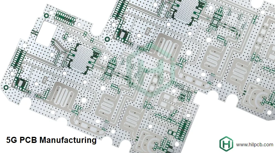
- A 5G AAU PCB should be reviewed as a dense RF, power, and thermal platform for an active antenna unit, not as a generic telecom motherboard.
- The first engineering checks are channel count, antenna path partitioning, RF material choice, power-delivery layout, thermal extraction, and manufacturable shielding strategy.
- Massive MIMO raises board complexity because RF chains, control logic, synchronization, and power stages have to coexist within tighter mechanical and thermal limits than a conventional radio board.
- Most failures come from weak channel isolation, inconsistent RF path control, poor PDN planning, trapped heat around PA sections, or late mechanical changes that break a previously valid layout.
- Early success usually depends on freezing stackup, RF zoning, heat path, and inspection strategy before the first build enters fabrication.
A 5G AAU PCB is the board set inside an active antenna unit that supports multiple RF chains, beamforming control, synchronization, power conversion, and antenna interfacing for 5G radio access equipment. The practical design problem is how to keep many RF and power paths working predictably together under high density, high heat, and tight mechanical packaging.
Contents
- What to review first on a 5G AAU PCB
- Key design and validation rule table
- Early engineering trade-off table
- How RF zoning and channel density affect layout
- How power delivery and thermal path affect stability
- What prototype and assembly teams should freeze before release
- FAQ
- Next steps
- References
- Author and review
What to review first on a 5G AAU PCB
An AAU is not just a radio board with more connectors. According to 3GPP's NTN and 5G evolution work and to mainstream O-RAN architecture practice, modern radio hardware has to support tighter coordination between RF chains, digital control, timing, and deployment constraints. In an AAU, that coordination happens under much higher channel density because the active radio and antenna functions are integrated more tightly.The first review points are usually:
- how many RF channels and antenna paths the unit must support and how they are partitioned physically
- whether the RF stackup, material family, and surface finish match the intended operating band and loss budget
- how PA sections, low-noise paths, control logic, and synchronization are isolated from one another
- whether the power-delivery network can support fast load changes without creating excessive noise or droop
- whether the thermal path out of PA, power, and shielding regions is defined before the mechanical envelope gets locked
For dense RF telecom layouts, it is usually worth aligning high-frequency PCB, high-speed PCB, and heavy copper PCB assumptions before release.
Key design and validation rule table
| Rule / parameter | What to check first | Why it matters | How to verify | If ignored | | --- | --- | --- | --- | --- | | RF channel partitioning | Freeze transmit, receive, control, and sync zoning early | AAU density makes late partition changes expensive and noisy | System block review and floorplan review | Crosstalk, awkward rework, shield failures | | Material and stackup fit | Choose RF material and stackup by band and loss budget | Wrong material choices can break insertion-loss and phase-consistency targets | Stackup review and coupon planning | Weak RF performance and unstable yield | | Power-delivery network | Review current paths, decoupling strategy, and rail segmentation | AAU boards often combine many dynamic loads in one compact assembly | Schematic review and bring-up test plan | Rail noise, voltage droop, intermittent faults | | Thermal path | Map heat out of PA, power, and dense shielded regions | RF sections can drift or degrade when heat is trapped | Thermal review and enclosure contact review | Hotspots, drift, shortened service margin | | Shielding and grounding | Define shield attachment, return paths, and partition boundaries | RF performance depends on physical containment, not only on schematic intent | Layout review and first-article inspection | EMI leakage and unstable channels | | Manufacturing test path | Decide how RF, power, and control behavior will be checked | Dense radio boards are hard to debug without planned access | DFT review and pilot checklist | Long debug loops and unclear root cause |Early engineering trade-off table
| Design choice | Usually stronger for | Main trade-off | What to confirm early | | --- | --- | --- | --- | | Hybrid RF + FR-4 stackup | Balancing RF performance and cost | Lamination and impedance control become more demanding | Band target, loss budget, fab route | | All-RF material stackup | Maximum RF control in critical paths | Higher cost and processing constraints | Whether the whole board really needs it | | Split RF and control boards | Cleaner partitioning and easier service in some platforms | More interconnect complexity and mechanical burden | Connector budget and enclosure space | | Integrated AAU board set | Tighter packaging and shorter signal path | Denser heat and shielding challenges | Thermal path and assembly route | | Thick copper power regions | Better current handling and heat spreading | Can complicate fine RF balance if applied indiscriminately | Current map and layer assignment | | Finer HDI breakout | Better density near control and support ICs | Stronger process discipline required | Package pitch, via strategy, rework path |How RF zoning and channel density affect layout
The biggest AAU layout mistake is treating all channels as copies of one another without respecting where isolation actually matters. High channel count is not only a routing problem. It is also a partitioning, shielding, grounding, and service problem.Three layout decisions usually matter most.
1. Keep RF paths short, predictable, and physically partitioned
AAU designs usually combine PA paths, receive paths, calibration paths, control buses, and timing distribution in one compact area. If zoning is vague, the board becomes harder to shield and harder to tune. For critical RF sections, high-frequency PCB and Rogers PCB planning usually needs to happen before routing starts.
2. Treat shielding as part of the layout, not as a late accessory
Shield cans, fence vias, grounding points, and keep-out geometry all change what is manufacturable. If they are added after routing is nearly complete, the result is usually compromised access and unstable EMI behavior. A PCB viewer or Gerber viewer review often catches these conflicts earlier than schematic review alone.
3. Plan inspection and rework before density closes the door
An AAU board can be electrically sophisticated and still be a bad production board if it has no realistic test access, shield removal plan, or inspection route. This matters even more when shielded RF blocks and power sections are tightly stacked.
How power delivery and thermal path affect stability
AAU boards put unusual stress on both the power-delivery network and the thermal design because many RF and support channels switch dynamically within a constrained space. The board should be reviewed as an RF-power-thermal system, not as separate subteams handing off isolated work.The main engineering checks are:
- whether high-current paths are separated cleanly from sensitive low-level control and receive paths
- whether local decoupling and rail segmentation support the actual switching behavior of the platform
- whether shielding strategy traps heat in exactly the areas where drift is least acceptable
- whether the enclosure and heat-extraction path are part of the PCB release review instead of being deferred to integration
If the design combines dense RF routing, power conversion, shielding, and mixed-package assembly, SMT assembly, turnkey assembly, and PCB prototype planning usually needs to move in parallel.
What prototype and assembly teams should freeze before release
AAU pilot risk usually drops when the release package includes both RF intent and production intent explicitly.A practical release checklist usually includes:
- RF zoning approved
Freeze PA, receive, control, sync, and antenna-interface regions before late mechanical edits start. - Material and stackup approved
Confirm the hybrid or RF-specific stackup against loss budget and fabrication route. - PDN review completed
Check rail segmentation, current paths, and local decoupling for the actual load profile. - Thermal extraction plan completed
Confirm heat spreading, enclosure contact, and shield impact before pilot release. - Shielding and inspection path documented
Define how shield install, inspection, test, and rework will be handled on the first build. - BOM review completed
Use a BOM viewer review to catch RF material, connector, PA, shield, and thermal-interface sourcing risk before procurement.
If the stackup or zoning is still moving, quick-turn PCB support is usually more valuable than rushing into a larger pilot.
FAQ
What makes a 5G AAU PCB different from a normal telecom board?
An AAU board has to support many RF chains, power stages, control paths, and antenna interfaces in one integrated unit, so zoning, shielding, thermal control, and PDN planning are much more tightly coupled.
Does every AAU board need RF laminate across the entire stack?
No. Many designs use hybrid stackups so only the layers that need stronger RF performance use specialty material. The right choice depends on the operating band and loss budget.
Why is thermal design so important on an AAU board?
Because PA and power regions can create local heating that changes RF behavior, reduces stability, and shortens service margin if the heat path is not planned early.
Is shielding mostly an EMI compliance issue?
No. Shielding is also a layout, grounding, manufacturability, and service issue. Weak shield planning can hurt RF stability long before formal compliance testing starts.
When should HDI be considered in a 5G AAU design?
Usually when control-side density, package escape, or mixed routing constraints make a conventional breakout too compromised.
Next steps
If you are developing a 5G AAU platform, the most useful next step is usually to review RF zoning, stackup, PDN layout, and heat extraction together before releasing the first prototype.HILPCB can support that process through:
- High-frequency PCB and Rogers PCB planning for critical RF layers
- High-speed PCB and HDI PCB support for dense control and support circuitry
- Heavy copper PCB review when current handling and thermal spreading are part of the same problem
- SMT assembly and turnkey assembly coordination for dense RF and shielded builds
- PCB prototype, quick-turn PCB, Gerber viewer, and PCB viewer for early validation
- Request a quote when your stackup, RF zoning, and assembly notes are ready