
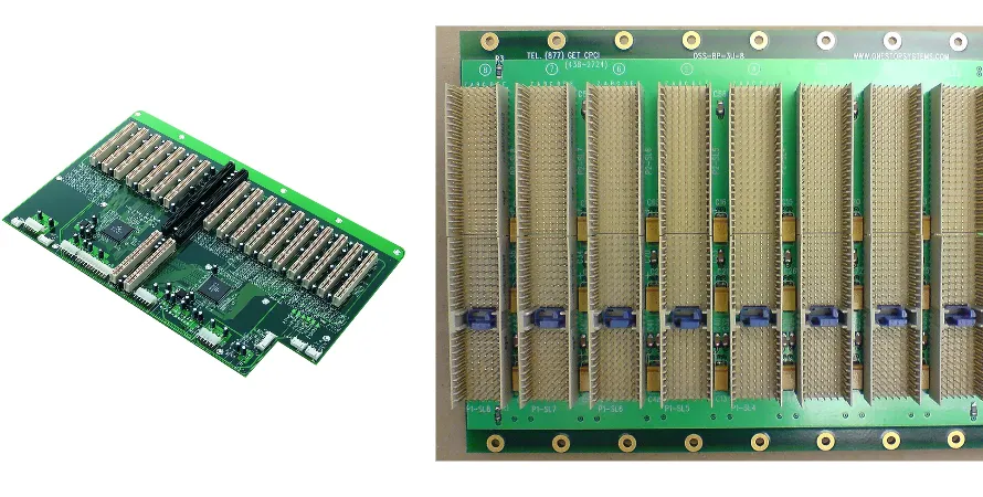
With the explosive growth of generative AI, LLM, and HPC, AI servers have become the core engine of modern data centers. The heart of these systems—the server motherboard and backplane PCB—now carries unprecedented data throughput and power density. As a compliance and reliability engineer responsible for long-term stability, I know that rigorous AI server motherboard PCB validation is no longer a late-stage checkbox. It is the foundation that determines whether an AI infrastructure succeeds or fails. A tiny signal distortion, an unaddressed hotspot, or an unstable power network can translate into million-dollar losses.
From a reliability engineering perspective, this article breaks down the complexity of validating AI server backplane PCB—spanning high-speed signal integrity (SI), power integrity (PI), thermal management, and mechanical reliability. We’ll look at validation strategies, precision test methods, and how partnering with an experienced manufacturer like Highleap PCB Factory (HILPCB) helps your backplane perform in harsh 24/7 environments. This is not just about passing tests—it’s about building a rock-solid hardware foundation for the next wave of AI.
Why AI server backplane validation is complex—and critical
Traditional server PCB validation focused on basic functionality and compliance. AI servers change the rules. The complexity is driven by three forces: extreme data rates, massive power consumption, and unprecedented integration density.
Exponential data-rate growth: AI workloads rely on real-time data exchange between accelerators (GPU/TPU) and between CPU, memory, and fabrics. High-speed interconnect standards such as PCIe 5.0 (32 GT/s), PCIe 6.0 (64 GT/s), and CXL are now baseline. At these speeds, loss, reflections, crosstalk, and jitter amplify dramatically—pushing PCB materials, stackup, and routing to near-limits.
Unprecedented power density: One AI accelerator can draw 700 W or more, and a single server chassis can exceed 10 kW. That current must be delivered precisely and stably through power planes. Any weakness in the PDN can cause IR Drop, EMI, or localized overheating—directly reducing performance and system stability.
Extreme design density: To shorten interconnect paths, AI server motherboards and backplane PCB are tightly packed. High layer counts (often 20+), HDI, complex BGA packages, and dense connector fields leave little physical margin. Density increases crosstalk and thermal challenges and demands higher manufacturing/assembly precision.
That’s why AI server motherboard PCB validation must be a system engineering effort that starts early and spans simulation, fabrication, assembly, and system-level testing—so electrical, thermal, and mechanical performance all meet spec.
Core challenges in high-speed SI validation
In AI servers, link reliability is the lifeline of performance. For high-speed serial buses like PCIe 5.0/6.0, SI validation is often the hardest part of the entire program. The goal is to preserve amplitude and timing accuracy from TX to RX across the full channel.
1. Channel loss budget control
Signals attenuate due to dielectric and conductor losses (insertion loss). A typical PCIe 5.0 channel budget is ~36 dB, which requires close alignment among designers, material vendors, and manufacturers. Key validation actions include:
- Material selection: use low-loss AI server motherboard PCB materials such as Megtron 6/7 and Tachyon 100G, with lower Dk/Df at GHz frequencies.
- Routing strategy: robust AI server motherboard PCB routing matters—trace length, width, via count, and via types all impact loss. Use TDR and VNA to measure S-parameters and confirm the channel stays within budget.
- Connector/via optimization: connectors and vias are primary discontinuities. Use 3D EM simulation (e.g., HFSS) to optimize geometry, and apply Back-drilling to remove via stubs to reduce reflections and loss.
2. Impedance control and matching
Differential impedance must be controlled tightly to the target (e.g., 85Ω or 100Ω) within ±7%. Any discontinuity causes reflections and degrades eye quality. Validation typically includes:
- Stackup design: precisely calculate trace geometry and spacing to reference planes.
- Manufacturing process control: manufacturers like HILPCB need advanced etching and lamination control to keep impedance consistent.
- Test verification: measure test coupons and on-board traces using TDR to confirm compliance. A strong AI server motherboard PCB layout plans impedance continuity from day one.
3. Crosstalk suppression
In dense routing regions, electromagnetic coupling between adjacent lines creates crosstalk and corrupts victim signals. Strategy:
- Simulation: use SI tools during layout/routing to predict NEXT and FEXT.
- Design rules: enforce spacing (3W/5W), optimize layer assignment, and prefer stripline structures where appropriate.
- Physical measurement: measure multi-port S-parameters with VNA to quantify real crosstalk.
PCIe Gen5 vs. Gen6: key SI validation parameters
| Parameter | PCIe 5.0 (32 GT/s, NRZ) | PCIe 6.0 (64 GT/s, PAM4) | Validation focus |
|---|---|---|---|
| Channel insertion loss budget | ~36 dB @ 16 GHz | ~32 dB @ 16 GHz (Nyquist) | Tighter requirements on material loss and connector performance. |
| Signaling | NRZ (non-return-to-zero) | PAM4 (4-level pulse amplitude modulation) | PAM4 is more sensitive to noise and nonlinearity; higher SNR is required. |
| BER target | 10-12 | 10-6 (pre-FEC) | Relies on FEC, but introduces new constraints on channel linearity and jitter. |
| Jitter & noise | Time-domain jitter (Tj, Rj, Dj) | More focus on SNR and vertical eye opening. | Requires higher-end scopes and analysis software for PAM4 eye evaluation. |
PI validation under AI workloads: what to verify
If SI is the data highway, PI is the power grid that drives it. In AI servers, accelerators like GPU can switch states fast and create >100 A current steps on the nanosecond scale. PI validation ensures supply voltage stays within tight tolerance under every load condition.
1. PDN impedance analysis
The PDN goal is low impedance across a wide band (DC to several GHz) to respond to transient load demands. Typical validation includes:
- Simulation-driven design: build a full PDN model from VRM to die early using PI tools and evaluate the impedance profile.
- Decoupling strategy: place and select capacitors across values and packages (bulk electrolytic to small MLCC) to suppress PDN impedance over frequency. ESL/ESR are key.
- Plane capacitance: use tightly coupled power/ground planes as board-level capacitance for a low-impedance HF noise path.
2. IR Drop and current density verification
High current flowing through copper generates voltage drop and heat. Focus on:
- Copper thickness and width: choose appropriate copper (including Heavy copper PCB) and trace width so IR Drop remains within spec (often 3–5%).
- Current density analysis: use simulation to find bottlenecks and hotspots in power paths and avoid copper fusing.
- Via current capacity: ensure via count and size can carry the required current.
Thermal validation: the foundation of long-term stability
Heat is the #1 reliability killer in electronics. In AI servers, kilowatts of power concentrate in tight volume. Thermal validation prevents throttling, premature aging, and catastrophic failure.
1. Hotspot identification and mitigation
- Thermal simulation (CFD): during design, use CFD with device power, PCB material properties, and cooling solutions (fans/heatsinks) to predict temperature distribution and find hotspots at VRM, processors, and high-speed transceivers.
- Physical measurement: on prototypes, use thermocouples and IR cameras under different workloads to verify simulation accuracy and cooling effectiveness.
2. PCB-level thermal design enhancements
- Thermal path optimization: add many Thermal Vias to conduct heat into internal copper planes or backside heatsinks quickly.
- Material selection: choose High-Tg materials to withstand higher operating temperatures without delamination or performance loss.
- Embedded cooling techniques: for extreme cases, consider embedded Copper Coin, heat pipes, or other advanced solutions.
A successful AI server motherboard PCB layout is always a co-optimization of electrical performance and thermal performance.
AI server PCB thermal KPI dashboard
Core device junction temperature (Tj)
< 105°C
Target: keep silicon within the safe operating area
VRM zone temperature
< 95°C
Target: maintain power efficiency and component lifetime
Peak PCB surface temperature
< 85°C
Target: prevent PCB aging and warpage
Connector temperature
< 70°C
Target: ensure connection reliability and signal integrity
Key steps in structural and mechanical reliability validation
AI server backplanes are typically large, high-layer, and heavy—and must survive frequent insertion cycles and transportation vibration. Mechanical validation ensures the PCB avoids structural failures across its full lifecycle.
- Warpage control: uneven copper distribution, poor stackup, or assembly process issues can cause warpage after reflow. Excess warpage impacts BGA solder quality and connector alignment. Validate via early simulation and post-build optical measurement.
- Connector insertion life: high-speed connectors must survive thousands of card insertions. Validate with cyclic insertion tests and check for mechanical and electrical degradation in the connector and solder joints.
- HALT/HASS: apply temperature/vibration stress well beyond normal operating range (HALT) to rapidly expose design/manufacturing weaknesses, then use HASS in production to screen early-failure risk units.
- Via reliability: vias experience Z-axis thermal stress in temperature cycling and can fatigue-crack. Validate via thermal shock testing (e.g., -40°C to 125°C) followed by microsection analysis of plating integrity.
From design to manufacturing: front-loading DFM/DFA in validation
The most effective validation starts at the earliest design stage. DFM (Design for Manufacturability) and DFA (Design for Assembly) bridge design intent and reliable physical production. In an AI server motherboard PCB validation workflow, early communication with an experienced manufacturer like HILPCB is critical.
- DFM checks: before release, the manufacturer reviews minimum line/space, drill sizes, pad geometry, solder mask openings, etc., to ensure the design fits process capability and avoids yield issues.
- Stackup and material guidance: based on SI/PI and thermal targets, HILPCB engineers can recommend the best low-loss AI server motherboard PCB materials and stackups to balance performance and cost.
- Assembly considerations: DFA checks whether placement supports SMT, soldering, and rework—e.g., avoid tall parts too close to BGA and reserve space for test probes.
A design optimized through DFM/DFA improves first-pass yield and reduces late validation surprises—especially important for fast iterations and time-to-market, and a prerequisite for AI server motherboard PCB quick turn.
🚀 AI server motherboard: an ideal path from simulation to full validation
For high-compute clusters, multi-dimensional simulation and co-manufacturing with HILPCB help ensure ultra-high-speed SI and system thermal reliability.
Define topology for protocols like PCIe 6.0; use end-to-end simulation to predict insertion loss and power-plane IR Drop.
Implement ultra-high-layer (20–30+ layers) HDI; strictly control diff-pair length match and via Backdrill parameters.
Align with HILPCB process standards and review warpage control for large panels, lamination alignment, and drill aspect-ratio limits.
Rapid prototyping with low-loss materials (e.g., Megtron 6/7); use automated test to complete FAI confirmation quickly.
Run eye validation under full load, IR thermal scanning, and airflow verification to ensure stable 7x24 compute output.
Best practices for automated test and fixture design (ICT/FCT)
For complex AI server motherboards with thousands of nodes, manual testing is impractical and inconsistent. Automated test is essential for both quality and throughput.
- ICT: ICT uses a bed-of-nails fixture to contact dedicated test points and quickly check soldering correctness (opens, shorts, wrong parts, polarity, etc.). Great Fixture design (ICT/FCT) is the key: it must align thousands of points precisely and provide stable contact.
- FCT: FCT simulates the real working environment of the PCB, applies inputs, and checks whether outputs match expectations. It validates functionality and performance under real load. FCT fixtures are more complex and often integrate power supplies, loads, signal generators, and measurement instruments.
- Boundary Scan (JTAG): for BGA pins that cannot be probed physically, Boundary Scan can access internal logic through a dedicated port and verify interconnect integrity—crucial for dense assemblies.
A complete strategy combines ICT, FCT, and Boundary Scan into a verification system spanning component-level through system-level validation. Professional Fixture design (ICT/FCT) ensures reliability and repeatability and is the core of mass-production quality control.
How HILPCB ensures excellent AI server backplane performance with advanced validation
Executing complex AI server motherboard PCB validation requires a strong and experienced manufacturing partner. With deep experience in High-Speed PCB and complex multilayer boards, HILPCB provides a one-stop solution from design support to final verification for AI server customers.
- Advanced manufacturing capability: HILPCB can build 50+ layer PCB, achieve 3/3 mil line/space, and hold ±5% impedance tolerance. Advanced Backdrill and HDI processes provide the physical foundation for strong SI.
- Comprehensive material inventory: we stock leading low-loss AI server motherboard PCB materials such as Rogers, Taconic, and Megtron, and recommend the optimal option based on application and cost targets.
- Strong test and validation equipment: we use Keysight VNA and TDR for accurate SI measurements and impedance verification. Our factory also runs AOI, X-Ray inspection (for BGA and PTH fill checks), and reliability labs for thermal shock and mechanical vibration testing.
- One-stop service: beyond PCB fabrication, we also provide Turnkey assembly—integrating DFM, DFA, and DFT into the full flow so every step is validated with strict quality control.
Common Questions
Why does AI server motherboard validation have to cover electrical, thermal, mechanical, and manufacturing factors together?
Because AI server reliability is determined by the interaction of all four domains, not by any single lab result. A board can pass an SI check and still fail later because of warpage, thermal hotspots, vibration sensitivity, assembly defects, or process drift, so validation has to be system-level from the beginning.
Which tests are most important when validating an AI server motherboard or backplane PCB?
The article highlights a layered strategy that combines SI tools such as VNA and TDR, manufacturing inspection such as AOI and X-Ray, automated electrical validation through ICT/FCT and Boundary Scan, and reliability stress work like thermal shock or vibration. Together these methods check both board correctness and long-term stability under real conditions.
Why are automated fixtures and a capable manufacturing partner so important in AI server PCB validation?
Because dense AI server boards cannot be validated repeatably with manual methods. Well-designed ICT/FCT fixtures, repeatable automated test flow, and a supplier that can connect DFM, fabrication, assembly, and reliability labs are what turn validation from a one-off success into a controllable production process.
Conclusion
AI server motherboard PCB validation is a cross-domain challenge spanning electrical, thermal, mechanical, and manufacturing disciplines. It demands a system-level mindset that builds reliability into every detail from the start—material choice, stackup planning, disciplined AI server motherboard PCB routing, tight process control, and comprehensive test strategy.
In today’s high-speed, high-power, high-density era, any weak link can collapse the system. With the structured validation approach described here and a capable partner like HILPCB, you can navigate these challenges and deliver stable, reliable, high-performance AI server hardware—forming a solid foundation for the future of AI.
If you’re launching your next AI hardware project and need a partner that understands and can solve these complex validation challenges, contact the HILPCB expert team. We look forward to building the next-generation computing foundation with you.