
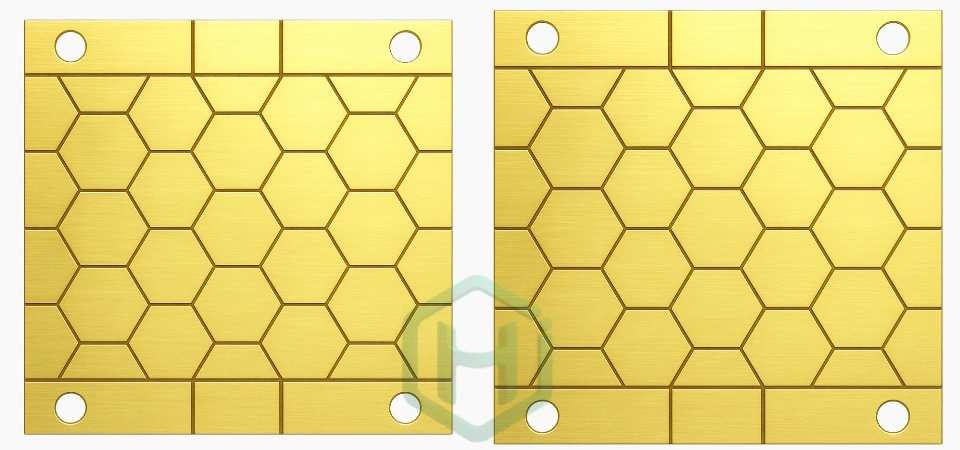
The rapid deployment of Silicon Carbide (SiC) and Gallium Nitride (GaN) power devices in Electric Vehicles (EV), renewable energy converters, and 5G base stations has created an unprecedented demand for substrates capable of extreme thermal management. Aluminum Nitride (AlN) ceramic PCBs are the only standard, non-toxic, commercially viable solution for these high-power, high-density applications, and understanding the foundations of advanced PCB manufacturing services can help contextualize these requirements.
For procurement managers and power electronics engineers, the choice of an AlN manufacturer is not a matter of simple cost-cutting; it is a critical reliability decision. A mediocre substrate can nullify the performance gains of SiC and GaN devices and introduce catastrophic thermal failure. This guide outlines the non-negotiable capabilities and quality checks required when selecting a long-term AlN manufacturing partner, complemented by insights from our professional ceramic PCB manufacturer guide.
I. Core Manufacturer Capabilities: Mastering AlN Bonding Technologies
The performance of an AlN PCB is fundamentally defined by the integrity of the copper-to-ceramic bond, which must minimize interfacial thermal resistance (often written as R_th) and withstand severe power cycling. A top-tier AlN manufacturer must demonstrate proven expertise in both Direct Bonded Copper (DBC) and Active Metal Brazing (AMB). Additional material context can be found in our high-performance ceramic PCB product portfolio.
Direct Bonded Copper (DBC) Quality Control
DBC offers a balance of performance and cost for moderate-to-high power applications. The primary manufacturing challenge on AlN is maintaining a void-free, uniform Cu/AlN interface. Supporting information about ceramic substrate structures can be found in our advanced ceramic circuit board technology overview.
Atmospheric precision – DBC bonding occurs at about 1065 °C in a precisely controlled N₂/O₂ atmosphere. The manufacturer must use state-of-the-art furnace technology with continuous gas analysis to keep the oxygen content within a tight 10–50 ppm window, preventing surface oxidation of the AlN substrate that causes poor bonding.
Copper thickness capability and uniformity – The ability to bond a wide range of copper thicknesses (typically from 100 µm to 600 µm) is essential. Thicker copper is needed for superior lateral heat spreading and higher current capacity, and it requires carefully tuned DBC process parameters to achieve uniform wetting and bonding across the entire panel.
Bond line inspection – A reputable manufacturer must use Scanning Acoustic Microscopy (SAM) as a standard Quality Assurance (QA) step on every production batch. SAM non-destructively maps the bond interface to detect internal voids and delamination. Your target supplier should guarantee a maximum allowable void percentage, typically less than 2% of the bonded area.
Active Metal Brazing (AMB): The Reliability Apex
AMB is required for the most demanding applications, such as EV traction inverters, where DBC bond fatigue life may be insufficient. The bond strength of AMB is inherently superior, often providing three to five times the power-cycling capability of DBC. A detailed breakdown of the AMB process can be reviewed in our advanced ceramic PCB manufacturing process guide.
- Vacuum brazing capability – This is mandatory. The manufacturer must possess high-vacuum brazing furnaces (base pressure below about 1 × 10⁻⁵ mbar) to execute the AMB process. This ensures the active metal (typically titanium, Ti) chemically reacts with the AlN to form a robust TiN interface, which is essential for superior thermo-mechanical stability.
- Brazing cycle control – Ask for typical brazing temperature, soak or hold time, and cooling profile. Precise control minimizes the formation of brittle intermetallic compounds (IMCs) at the interface, which can otherwise compromise long-term reliability.
- Mechanical integrity verification – AMB bond strength must be verified via destructive pull or peel tests on test coupons, with results that typically exceed 30 N/mm². A serious supplier will share representative test reports rather than generic marketing promises.
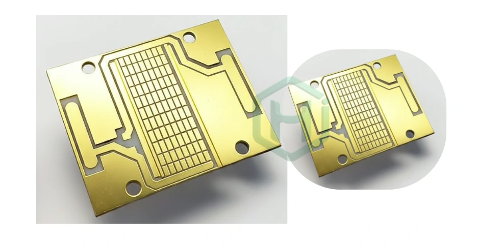
II. Procurement Decision Matrix: Cost, DFM, and Lead Time
Sourcing AlN PCBs is a strategic purchasing function. You must compare not just unit price, but the total cost of ownership, which also includes failure risk, qualification cost, and time-to-market impact.
Managing Lead Time and Production Scale
AlN fabrication is inherently slower than organic PCB production because it involves high-temperature processing steps (sintering, bonding) and specialized laser machining.
| Production Stage | Typical Lead Time | Manufacturer Capability Assessment |
|---|---|---|
| Raw substrate sourcing | 4–8 weeks | Does the supplier hold inventory of high-purity AlN? Are they dual-sourced for critical materials? |
| Prototyping / NPI | 4–6 weeks | Should be comparable to small batch assembly lead times, requiring flexible laser programming and quick tooling changes. |
| Mass production | 8–12 weeks | Requires multiple DBC and AMB furnaces plus automation in laser machining, plating, and inspection lines. |
| Turnkey assembly | +3–4 weeks | Ability to integrate AlN substrates into a full module, including die attach, wire bonding, and heatsink or baseplate assembly. |
Sourcing strategy:
For New Product Introduction (NPI), prioritize a manufacturer with rapid laser-processing capability and short setup times so that small runs can be turned around quickly. For large volume production, verify the installed base of bonding furnaces and automation to guarantee large volume assembly capacity without bottlenecks.
Cost Drivers and Value Analysis
AlN PCBs are significantly more expensive than Al₂O₃ ceramics or standard MCPCBs. A useful comparison resource for organic PCB alternatives is our FR4 PCB solutions.
Material purity – Cost escalates with AlN purity (and thus thermal conductivity). High-purity material with thermal conductivity above 200 W/(m·K) is a major cost factor but may be required for extreme power density.
Bonding process choice – In terms of cost, AMB is more expensive than DBC, which in turn is far more expensive than thick-film metallization. AMB requires specialized vacuum equipment and high-cost braze alloys, but it delivers much better fatigue life.
Dimensional complexity – Complex laser-machined features such as small vias, non-rectangular or highly contoured outlines, and high aspect-ratio edges significantly drive up unit costs due to longer processing time and lower yield.
Testing requirements – SAM scanning, thermal cycling tests, and extended burn-in add to the cost per board but are essential for high-reliability projects. Never compromise on critical testing simply to reduce the quoted price.
Design for Manufacturability (DFM) Consultation
A superior AlN manufacturer will provide proactive DFM consultation to prevent costly redesigns and field failures later.
- Stress-mitigation review – The manufacturer should analyze your layout for potential thermal stress hotspots (for example, at the corners of large copper pads) and recommend copper-relief features such as slots, trenches, or rounded inner corners to reduce stress concentration.
- Material utilization – They should advise on optimal panelization and nesting to maximize use of the expensive AlN substrate material, directly reducing waste and cost without changing the electrical design.
- Interconnect optimization – You should receive guidance on when to use filled laser vias versus edge connections or external bus bars to balance current capacity, thermal performance, and manufacturing yield.
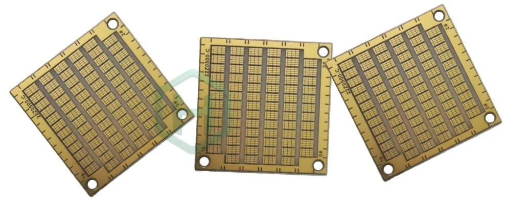
III. AlN Applications and Reliability Assurance
AlN PCBs are foundational technology for applications where failure is catastrophic or extremely costly. The manufacturer’s certification and testing protocols must reflect this high-stakes environment.
Automotive Electronics and IATF 16949
For EV and hybrid vehicle power modules (traction inverters, DC/DC converters, and on-board chargers, or OBCs), AlN must meet the highest automotive quality standards.
IATF 16949 certification – This is a non-negotiable requirement for any supplier targeting the automotive market. It signifies a robust Quality Management System (QMS) focused on continuous improvement, variation reduction, and defect prevention in serial production.
Power-cycling validation – AlN boards must be validated against thousands of thermal power cycles (temperature swing, often written as ΔT) that simulate real-world driving profiles. A reputable supplier will provide quantitative data showing the Weibull distribution and the characteristic life (Nη) of their substrates under your specified cycling conditions.
AEC-Q100 component compatibility – Ensure the manufacturer understands the requirements for mounting and bonding AEC-Q100 qualified SiC or GaN bare dies onto their AlN substrate, including specialized high-reliability die-attach processes such as pressure-assisted silver sintering.
RF, Radar, and High-Frequency Modules
In 5G and upcoming 6G base-station power amplifiers (PAs) and AESA radar systems, AlN is selected for its excellent thermal properties combined with low RF signal loss.
Low dielectric loss (loss tangent) – The manufacturer must guarantee the AlN substrate’s low loss tangent (tan δ ≤ 0.0005) to minimize signal attenuation in GHz-range applications.
Thin-film precision – For high-frequency modules, thin-film metallization on AlN (using sputtering and photolithography) is required to achieve ultra-fine lines around 10 µm and the smooth surface finish needed for low conductor loss due to skin-effect behavior. Verify their cleanroom class and lithography equipment resolution.
Thermal stability – AlN substrates help prevent RF output power and phase from drifting with temperature in GaN HEMT devices, which is a key performance indicator for radar and communications systems.
Quality Assurance and Traceability
High-value AlN components require full traceability from raw powder through to the finished board.
- Material traceability – The manufacturer must be able to trace each finished AlN substrate back to the original powder batch and its Certificate of Analysis (COA), including purity (typically ≥ 99%) and initial thermal-conductivity K value.
- Final inspection standards – All finished AlN boards should undergo 100% Automated Optical Inspection (AOI) and a robust Dielectric Withstand Voltage (DWV) test to confirm electrical isolation at the specified high operating voltage.
IV. Full-Service Capabilities in Advanced Ceramic PCB Manufacturing
Modern power electronics and high-reliability systems increasingly require ceramic PCBs that combine material flexibility, stable volume production, and dependable long-term performance. Selecting a manufacturer with complete in-house capabilities ensures consistent quality from prototype through series production, which aligns with the broader capabilities highlighted in our multilayer PCB production capabilities.
At HILPCB, our engineering team supports a wide range of ceramic substrates—including AlN, Al₂O₃, and Si₃N₄—with scalable manufacturing processes and optional turnkey assembly for fully integrated module delivery.
Key Manufacturing and Support Capabilities
- Multi-Material Ceramic PCB Production:
Capability to fabricate AlN, alumina, silicon nitride, multilayer ceramics, and thick-film structures for diverse power, RF, and industrial applications. - Prototype-to-Mass Production Scalability:
Standardized AMB/DBC processes, equipment redundancy, and stable process control ensure consistent thermal and electrical performance across all production volumes. - Turnkey Assembly Services:
Optional die attach, silver sintering, soldering, heavy wire bonding, heatsink integration, and final electrical/thermal testing to streamline module-level manufacturing. - Long-Term Technical Support:
Ongoing material guidance, process recommendations, reliability documentation, and assistance with failure analysis throughout the product lifecycle. - Design-Stage Collaboration:
Engineering support for stack-ups, metal thickness selection, thermal interface planning, and layout considerations to improve overall system reliability.
Partner with our experts, a leading AlN ceramic PCB manufacturer, to secure a supply chain built on validated thermal reliability, robust process control, and industry-leading quality standards from prototype through series production.
Common Questions
Why choose an AlN PCB instead of standard substrates?
Because AlN combines very high thermal conductivity with electrical insulation and suitable dielectric performance. It is often selected when FR-4, MCPCB, or lower-performance ceramics cannot remove heat fast enough or keep power and RF modules stable.
Why do thermal conductivity and dielectric performance matter together in AlN PCB design?
Because many power and RF applications need both efficient heat extraction and controlled electrical behavior. A substrate that only solves heat but introduces higher loss or instability can still limit efficiency and long-term reliability.
Why are process control and material traceability critical for AlN PCBs?
Because AlN boards are usually used in high-value, high-reliability systems where bonding quality, substrate purity, insulation strength, and thermal cycling life must remain consistent. Traceability and testing help catch variation before it becomes a field failure.
Why does full-service ceramic PCB capability matter for AlN projects?
Because AlN programs often depend on coordinated substrate fabrication, metallization, joining, assembly, and reliability verification. A supplier that supports the full flow reduces handoff risk from prototype through volume production.