
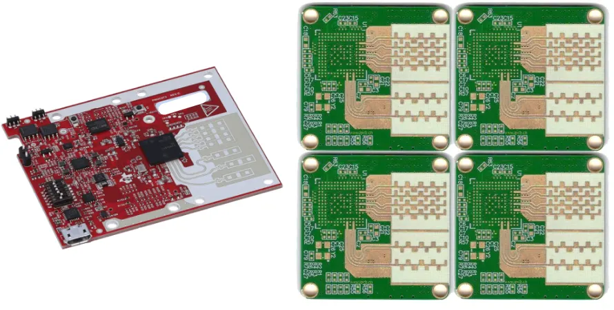
- An antenna analyzer PCB should be reviewed as a precision reflection-measurement path, not just as a small RF board with a display and connector.
- The first checks are frequency range, impedance reference, directional-coupler accuracy, detector or receiver path, calibration method, and connector-launch quality.
- Most failures show up as unstable VSWR, wrong return-loss readings, drifting impedance plots, or measurements that change too much with cables, adapters, or grounding.
- Material choice matters on higher-frequency designs, but coupler layout, reference planes, calibration standards, and port transitions usually dominate accuracy first.
- Prototype success depends on freezing the calibration and fixture assumptions before the first hardware build is judged.
An antenna analyzer PCB is a board that generates or routes a swept RF stimulus to an antenna or transmission line and measures the reflected response so impedance, return loss, and VSWR can be derived. Because those values depend on small differences in amplitude and phase, the PCB has to preserve launch quality, coupling accuracy, grounding, and calibration integrity.
Contents
- What to review first on an antenna analyzer PCB
- Key design and validation rule table
- Early engineering trade-off table
- How coupling, calibration, and RF layout affect measurement credibility
- How measurement setup should be planned
- What prototype teams should lock down before release
- FAQ
- Next steps
- References
- Author and review
What to review first on an antenna analyzer PCB
An antenna analyzer has to do more than generate RF energy. It has to separate incident and reflected behavior in a way that remains stable across the intended frequency range. That means the PCB is part of the measurement system itself, not just part of the enclosure.The first review points are usually:
- what frequency range, impedance reference, and accuracy target the analyzer is expected to support
- whether the architecture is based on scalar detection, vector-style measurement, or a simplified hybrid approach
- how the directional coupler, bridge, or detector path is implemented and isolated
- whether port launches, connector choice, and grounding preserve a clean 50 ohm reference
- how open, short, load, and any fixture or cable calibration will be performed and repeated
For GHz-range analyzer boards, it is usually worth comparing high-frequency PCB and Teflon PCB options before stackup and launch geometry are frozen.
Key design and validation rule table
| Rule / parameter | What to check first | Why it matters | How to verify | If ignored | | --- | --- | --- | --- | --- | | Frequency and accuracy fit | Match the architecture to the real sweep range and error budget | Coupler, detector, and board loss behavior change with range | System review and block-level RF review | Credibility falls apart at band edges | | Calibration strategy | Define how open, short, load, and any fixture compensation will work | Calibration determines whether readings are portable and repeatable | Calibration flow review and lab procedure review | Good-looking plots with poor traceability | | Port and launch quality | Treat the test port and connector as part of the DUT plane | Weak launches corrupt return-loss and impedance readings | Layout review and [Gerber viewer](/tools/gerber-viewer/) inspection | Cable swaps appear to change the antenna more than it really changed | | Coupler or bridge behavior | Keep coupling ratio, directivity, and isolation believable over frequency | Reflection measurements depend on separating forward and reflected energy cleanly | Simulation review and bench validation plan | VSWR and return loss become unstable | | Grounding and shielding | Keep receiver and detector sections away from digital and display noise | Sensitive RF detection paths can be corrupted by local coupling | Layout zoning and shield review | Drift, repeatability loss, and noisy traces | | Measurement reference control | Freeze adapters, cables, and calibration plane assumptions | The measurement plane is meaningless if the setup changes each time | Fixture checklist and calibration notes | Lab data cannot be compared across revisions |Early engineering trade-off table
| Design choice | Usually stronger for | Main trade-off | What to confirm early | | --- | --- | --- | --- | | Simpler scalar architecture | Lower cost and simpler embedded implementation | Less phase-rich insight and lower flexibility | Real measurement objective | | More vector-like measurement path | Better impedance and reflection interpretation | More RF and calibration complexity | Processing path and calibration burden | | Board-edge port launch | Shorter path to the DUT connector | Tighter enclosure and grounding constraints | Mechanical and shield plan | | Extra shielding and via fences | Better repeatability and less internal coupling | More area, cost, and rework difficulty | Service access and enclosure fit |How coupling, calibration, and RF layout affect measurement credibility
Antenna analyzers are often judged by their screen output, but their real value depends on whether the reading stays trustworthy when the board, cable, and calibration setup are repeated. PCB design is central to that trust.Three review questions usually matter most.
1. Is the measurement plane defined clearly?
If the team cannot say exactly where the calibration plane is, then impedance and return-loss data will be argued over later. The connector, adapter, cable, and any fixture have to be treated as part of the measurement definition.
2. Is the reflection path separated cleanly enough?
The analyzer only works if forward and reflected behavior are separated predictably. Weak directivity, poor port launches, or noisy detector routing can make the antenna look worse or better than it really is.
3. Is the layout stable enough to support calibration?
Open, short, and load standards are only useful when the surrounding PCB structure is stable. For denser RF layouts, Rogers PCB and high-frequency PCB review often matters more than adding extra DSP after the fact.
How measurement setup should be planned
An antenna analyzer project is not ready when the PCB routes correctly. It is ready when the team can explain how the instrument will be calibrated and what must stay constant during verification.The most common setup questions are:
- whether the analyzer will be validated against a VNA, reference loads, or known antenna standards
- whether open, short, load, and any through or fixture compensation steps are defined before prototype arrival
- whether cable movement, adapter choice, and enclosure state are controlled during comparison testing
- whether the instrument must prove only scalar values such as VSWR and return loss or also more detailed impedance behavior
If the project still needs quick hardware loops, PCB prototype, quick-turn PCB, and SMT assembly planning usually saves more time than debating calibration after assembly is complete.
What prototype teams should lock down before release
The first prototype should prove the measurement method, not just the firmware UI. Before release, the team should know which accuracy questions the build is supposed to answer.A practical release checklist usually includes:
- Measurement range frozen
Define the intended sweep range, impedance reference, and required output metrics such as VSWR, return loss, or Smith-chart behavior. - Calibration flow approved
Freeze the open, short, load, and any fixture or cable compensation process that the lab will use. - Port and launch design approved
Confirm connector family, reference-plane geometry, and enclosure interaction before fabrication. - Reference hardware identified
Decide what known standards, loads, or antennas will be used to judge the first build. - Revision and assembly assumptions recorded
Keep BOM, shielding parts, stackup, and detector-path notes aligned. A BOM viewer review helps prevent unnoticed substitutions in RF-critical builds.
FAQ
What is the first thing to check on an antenna analyzer PCB?
Start with the measurement range, calibration plane, and the reflection-measurement architecture. Those choices usually determine whether the rest of the board can deliver believable impedance results.
Why can antenna analyzer readings change a lot when the cable or adapter changes?
Because the cable and adapter can shift the effective measurement plane. If calibration and fixture assumptions are not controlled, the setup itself changes the result.
Is return loss the same thing as VSWR?
No. They describe the same mismatch behavior differently. Return loss is a logarithmic reflection measure in dB, while VSWR expresses the standing-wave ratio on the line.
Why do open and short standards not always appear as perfect points on a Smith chart?
Because real calibration standards are modeled physical structures, not perfect mathematical ideals. Their electrical length and parasitics are part of the calibration model.
What should be frozen before the first prototype release?
Freeze the sweep range, calibration process, connector and launch design, comparison standards, and the exact hardware revision that will be evaluated.
Next steps
If you are building an antenna analyzer or another RF reflection-measurement board, the most useful next step is usually to review calibration plane, coupler behavior, connector launch, and grounding as one system.HILPCB can support that process through:
- High-frequency PCB planning for couplers, bridges, and detector paths
- Teflon PCB and Rogers PCB review when dielectric stability matters
- SMT assembly support for compact RF and mixed-signal builds
- PCB prototype and quick-turn PCB support for early validation hardware
- Request a quote when your RF path, calibration flow, and build package are ready for review