
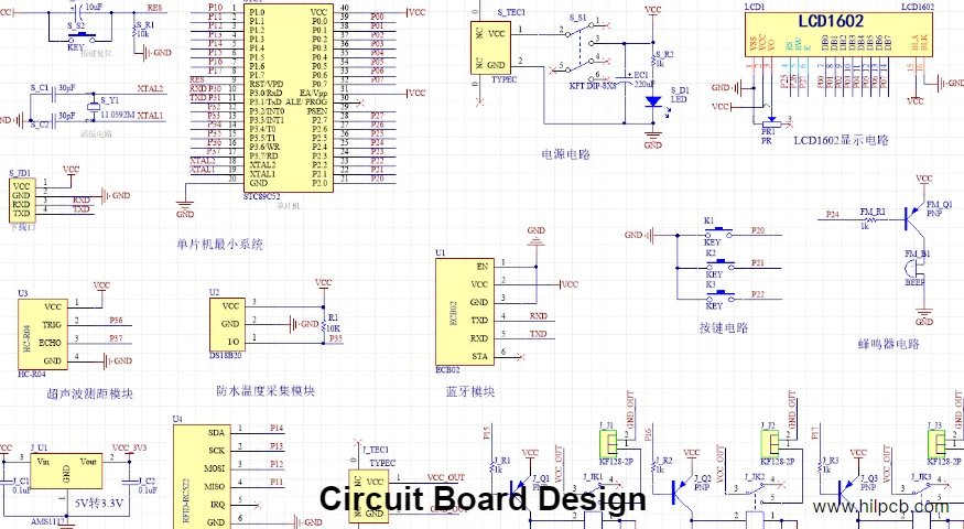
In high-speed digital design, the clock is the “heart” of the system. A stable and accurate Clock Tree layout is the foundation for data synchronization and overall system reliability. Yet from stackup decisions and routing details to manufacturing handoff, engineers routinely run into tricky problems. Centered on clock tree layout tutorial, this guide organizes 20 of the most common PCB design FAQs and provides end-to-end explanations—from symptoms and root causes to fixes and prevention actions.
Whether you’re a beginner or an experienced engineer, this all-in-one guide (including a DFM checklist and a recommended learning path) helps you build a more robust design baseline and reduce volume-production risks.
FAQ quick overview table
To help you locate issues quickly, here is a summary table covering the key topics discussed in this article.
| # | Topic | Key metric | Quick fix |
|---|---|---|---|
| 1 | Impedance control failure | Impedance error > ±10% | Verify stackup parameters, trace width, and copper thickness match the simulation |
| 2 | Reference plane discontinuity | Signal crosses a split | Add GND via stitching/bridging, or reroute |
| 3 | Fiberglass weave effect | Timing jitter increases | Use Zig-Zag routing or select low-Dk spread-glass styles |
| 4 | Stackup selection | SI vs. cost | Prefer symmetric structures with paired GND/Power planes |
| 5 | Chaotic module placement | Critical paths too long | Follow “signal flow” and shorten high-speed links |
| 6 | Differential mismatch | Phase error > 5 ps | Tune serpentine; keep intra-pair length match within ±2 mil |
| 7 | Via impedance discontinuity | Reflections / attenuation | Optimize via geometry; remove unused pads (Back-drilling) |
| 8 | Broken return path | EMI exceeds limits | Ensure continuous reference planes under every signal |
| 9 | Clock topology issues | Clock skew too large | Use H-Tree or star topology; keep branches equal length |
| 10 | Excessive stub | Ringing | Keep stub length < (Tr / 6) * v |
| 11 | Serpentine side effects | Coupling / impedance variation | Keep meander spacing > 3W; bend angle ≥ 135° |
| 12 | Poor decap placement | Power noise | Place near pins; route through the cap before the pin |
| 13 | Large power-loop area | Higher radiated emission | Minimize the loop formed by decap + IC power/ground pins |
| 14 | Overusing split ground | Cross-region EMI | Use a solid ground plane unless isolation is required |
| 15 | Crosstalk | Neighbor signal distortion | Spacing > 3W (trace width), or add ground isolation |
| 16 | Ground bounce | Digital logic errors | Add more ground vias; ensure low-impedance return paths |
| 17 | Incomplete DRC rules | Low yield | Update DRC based on fab capability and cover all critical rules |
| 18 | Manufacturing data mismatch | Gerber/BOM/XY conflicts | Use a single source of truth; version control; cross-check before release |
| 19 | Uncontrolled design changes | New rev reintroduces issues | Use an ECN process; run full regression after changes |
| 20 | Missing impedance coupon | Process cannot be validated | Add impedance test coupons explicitly in the Gerber set |
Stackup & impedance
The stackup is the “skeleton” of the PCB—it directly determines impedance and signal integrity.
Question: Why does measured impedance deviate from the design value by more than 10%?
- Symptoms: TDR shows a 50Ω single-ended trace measuring 58Ω, or a 90Ω differential pair measuring 105Ω—causing severe reflections.
- Root causes:
- Wrong stackup inputs: dielectric thickness and Dk/Df values in the design don’t match the materials actually used by the fab.
- Incorrect etch compensation: fab etch compensation differs from the EDA presets.
- Copper thickness variation: base copper plus plating results in a higher total copper thickness than expected.
- Solutions:
- Confirm materials with the fab early: get their preferred laminates, prepreg options, and real Dk/Df values at the start.
- Define manufacturing tolerances: request tolerance ranges for trace width, lamination thickness, etc.
- Use professional tools: Polar Si9000, or HILPCB’s free stackup simulation service, to calculate with the fab’s real parameters.
- Prevention checklist:
- Include a detailed stackup drawing in the design file: layer materials, thickness, Dk, etc.
- Attach stackup fabrication notes with the Gerber package.
- Require an engineering confirmation (EQ) of the stackup before fabrication.
Question: What happens if a high-speed signal crosses a split reference plane?
- Symptoms: random crashes under high-throughput tests, or EMI failures at specific frequencies.
- Root cause: when a trace crosses a split in GND or Power, the return current is forced to detour, creating a large loop. That loop behaves like an antenna—radiating EMI and injecting noise.
- Solutions:
- Avoid routing across splits: adjust placement so high-speed traces remain above a continuous reference plane.
- Add bridging capacitors/vias: when unavoidable, place a 0.1uF capacitor (Power-to-GND split) or a group of GND stitching vias (GND-to-GND split) at the boundary to provide a low-impedance “bridge” for return current.
- Prevention checklist:
- Identify all high-speed nets during floorplanning and plan their routes and reference planes.
- Use EDA SI analysis to check return-path continuity.
- Explicitly prohibit high-speed signals from crossing plane splits in internal design rules.
Question: What is the fiberglass weave effect, and how does it affect clocks?
- Symptoms: for differential signals above 10Gbps, eye opening degrades and jitter increases, raising BER.
- Root cause: FR-4 is made of glass weave and epoxy resin. Glass (Dk ≈ 6) and resin (Dk ≈ 3) have different dielectric constants. If one line of a differential pair rides mainly over glass bundles while the other rides mainly over resin, the effective Dk differs, causing propagation delay mismatch and phase imbalance.
- Solutions:
- Zig-Zag routing: route at a small angle (e.g., 10–15°) so the trace alternates across glass and resin regions, averaging the effective Dk.
- Use better glass styles: Mechanically Spread Glass or Flat Glass weaves provide more uniform construction.
- Rotate the placement: rotate the entire design or critical blocks by an angle before routing.
- Prevention checklist:
- For ≥10Gbps signals, define the routing strategy (e.g., Zig-Zag) in the design standard.
- During material selection, evaluate whether higher-performance laminates (e.g., Megtron 6, Rogers 4350B) are necessary.
Question: How do you choose a suitable stackup for high-speed clocks?
- Symptoms: severe EMI, or key clock signal quality fails requirements after design completion.
- Root cause: an improper stackup leads to poor reference planes and strong interlayer coupling—for example, placing two high-speed signal layers adjacent without a ground plane in between.
- Solutions:
- Symmetry: keep the stackup as symmetric as possible to reduce warpage during thermal processing.
- Solid reference planes: each high-speed signal layer should be adjacent to a solid GND or Power plane. Use microstrip (outer layer) or stripline (inner layer) structures.
- Tightly coupled power/ground: tightly couple Power and GND planes (e.g., spacing ≤ 4 mil) to form an inherent plane capacitor and a low-impedance PDN.
- Prevention checklist:
- Prefer classic stackups such as
SIG-GND-PWR-SIGorGND-SIG-SIG-GND. - Read the pcb stackup tutorial for more best practices.
- Treat stackup planning as a top priority at project kickoff.
- Prefer classic stackups such as
Layout & routing
Placement determines whether your signal paths are inherently good; routing turns design intent into reality.
Question: How do you do modular placement to optimize clock-tree performance?
- Symptoms: clock routes from source to receivers are too long and complex; skew and jitter are hard to control.
- Root cause: placement doesn’t follow “signal flow”. Critical devices (CPU/FPGA/DDR) are scattered, causing the clock distribution network to become tangled.
- Solutions:
- Identify critical paths: confirm the clock source (crystal/PLL) and all critical clock sinks.
- Center the core: place the clock source or the main logic core (e.g., FPGA) near the PCB center.
- Group by function: cluster clock-synchronous devices (DDR, high-speed interface ICs) close to the core to form functional islands.
- Prevention checklist:
- Do an initial placement plan already in the schematic stage.
- Draw a signal-flow diagram so paths from input to output are shortest and most direct.
- Place clock networks and other high-speed critical nets (DDR, etc.) first, then place low-speed circuitry.
Question: How strict is length matching for differential clock pairs?
- Symptoms: the differential eye crossing shifts, and common-mode noise rejection degrades.
- Root cause: P/N length mismatch introduces phase error at the receiver, converting part of the differential signal into common-mode.
- Solutions:
- Tight intra-pair match: for high-speed differential clocks (PCIe, SATA), keep intra-pair mismatch within ±2 mil.
- Symmetric routing: keep P/N symmetric; avoid unequal delay from bends/vias.
- Final phase tuning: do the final length tuning near the receiver (e.g., FPGA) to align phase at the pins.
- Prevention checklist:
- Set strict differential-pair rules in the EDA tool.
- Avoid placing test points or components on only one side of the pair.
- When using serpentine compensation, keep coupled meander sections under 1/3 of the total length.
Question: How much do vias affect high-speed clock signals?
- Symptoms: slower edges after via transitions; reflections and ringing become obvious.
- Root cause: standard via structures (pad/barrel/anti-pad) add parasitic capacitance and inductance, creating impedance discontinuities. A typical through-hole via can be 10–15Ω lower impedance than the transmission line.
- Solutions:
- Optimize via geometry: reduce pad and anti-pad sizes to lower parasitic capacitance.
- Add ground vias: place one or more GND vias next to the signal via so the return path remains continuous and the impedance step is reduced.
- Back-drilling: for very high speeds (>10Gbps), remove the unused via stub to eliminate resonances.
- Prevention checklist:
- Minimize layer transitions for high-speed clocks.
- Define different via styles for different signal classes in design rules.
- Follow via guidance in the high speed trace routing guide.
Question: What is the return path, and why is it critical for clocks?
- Symptoms: EMI fails even though traces are short; nearby low-speed nets get disturbed.
- Root cause: engineers often focus on the forward path and ignore the return. At high frequency, return current follows the lowest-impedance path—typically right under the trace on the adjacent reference plane. If that path is cut or elongated, the return current detours, forming a large loop and radiating strongly.
- Solutions:
- Ensure continuous reference planes: keep a continuous, un-split GND or Power plane under the trace.
- Provide reference transfer at layer changes: when changing layers, add nearby ground vias so the return can “jump” between reference planes smoothly.
- Prevention checklist:
- After routing, highlight the clock nets and verify reference planes beneath are intact.
- Use ground plane best practices and prefer solid ground planes.
Question: How do you design a low-skew clock tree?
- Symptoms: sampling errors on parallel interfaces (e.g., DDR buses) because the clock arrival time differs across loads.
- Root cause: large differences in physical path length from the clock source to each load create different propagation delays.
- Solutions:
- H-Tree topology: for many identical loads (e.g., FPGA clock networks), H-Tree can physically guarantee equal branch lengths.
- Star topology: fan out from a Clock Buffer to each load, then tune each branch length individually.
- Daisy-chain: only suitable for low-speed applications with relaxed timing; not recommended for high-speed clocks.
- Prevention checklist:
- Decide the clock-tree topology early in the project.
- Use EDA length-matching to control all clock branches precisely.
Question: What’s the risk of stubs on signal traces, and how do you control them?
- Symptoms: severe ringing; even double clocking.
- Root cause: T-branches or unterminated segments form a stub. When the signal hits the stub end, it reflects fully; the reflection adds back into the main signal and distorts the waveform.
- Solutions:
- Control stub length: a practical rule is stub length (inches) should be less than half the rise time (ns). A more accurate formula:
L_stub < (Tr / 6) * v, whereTris rise time andvis propagation velocity in the dielectric. - Avoid T-branches: for high-speed clocks, use daisy-chain or star from the source and avoid mid-route forks.
- Control stub length: a practical rule is stub length (inches) should be less than half the rise time (ns). A more accurate formula:
- Prevention checklist:
- Set a maximum allowed stub length in routing rules.
- Review topology for all high-speed networks.
Need a professional clock-tree layout review?
An uncertain clock-tree design can lead to weeks of debugging and expensive respins. HILPCB’s high-speed PCB experts can provide a comprehensive design review—from stackup planning and impedance simulation to key-net topology analysis—so your first fabrication run succeeds. We also offer free impedance coupon design and validation.
Get a free design reviewPower & EMC
Clean power and solid EMC performance are essential to system stability.
Question: Beyond length matching, what side effects can serpentine routing introduce?
- Symptoms: after using serpentine tuning, insertion loss increases, or differential performance degrades.
- Root causes:
- Impedance discontinuity: bends change effective trace width and the distance to the reference plane, causing local impedance variation.
- Intra-pair coupling changes: if meander segments are too close, extra coupling is introduced, hurting differential balance.
- Extra delay: excessive meandering adds delay beyond the straight-line physical estimate.
- Solutions:
- Use gentle bends: keep bend radius > 3W (R > 3W) and segment spacing > 3W.
- Symmetric compensation: for differential pairs, add meanders symmetrically to P/N, or keep compensation centered within the pair.
- Prevention checklist:
- Prefer global path tuning first; use serpentine only for final fine adjustment.
- Limit max amplitude and min spacing for serpentine in design rules.
Question: How should decoupling capacitors be placed for maximum effectiveness?
- Symptoms: even with enough decaps, the power rail of a high-speed IC still has significant noise.
- Root cause: poor placement creates excessive parasitic inductance. High-frequency current always follows the lowest-impedance (lowest-inductance) path.
- Solutions:
- Place close: put the capacitor as close as possible to the IC power and ground pins.
- Optimize the path: the current path should go through the capacitor pads before reaching the IC pins.
- Multiple vias to ground: use multiple vias from the capacitor ground terminal to the GND plane to reduce inductance.
- Value mix: combine values (1uF, 0.1uF, 0.01uF) to cover a wider noise spectrum.
- Prevention checklist:
- Create decap footprints with optimized via patterns in the library.
- Follow the IC datasheet’s decap layout recommendations.
Question: How do you understand and minimize power-loop area?
- Symptoms: failures in radiated emission (RE) tests, especially at clock harmonics.
- Root cause: high-frequency currents flowing in a loop (IC power pin -> decap -> IC ground pin -> GND plane -> Power plane -> IC power pin) form an efficient radiator. Larger loop area means stronger radiation.
- Solutions:
- Compact placement: place decaps right next to the IC power/ground pins.
- Use planes for power: use solid Power/GND planes rather than long traces to supply high-speed ICs. Tight plane coupling yields the minimum loop area.
- Prevention checklist:
- During layout review, focus on the decap loops of all high-speed ICs.
- Read what is controlled impedance pcb to understand how plane layers help control loop area.
Question: Is a split ground plane good or bad?
- Symptoms: to isolate analog and digital circuits, a split ground is used, but noise coupling between regions becomes worse.
- Root cause: while split ground can isolate low-frequency noise, if high-speed traces cross the split, the return path detours and creates severe EMI. Also, the two ground regions can develop significant potential differences.
- Solutions:
- Prefer a unified ground: for most mixed-signal designs, use a single solid ground plane and isolate via placement partitioning (analog vs. digital), not by physically cutting the plane.
- Single-point bridge: if a split is mandatory, connect at the boundary with a ferrite bead or 0Ω resistor to provide a controlled return path for cross-region signals.
- Prevention checklist:
- Consider split ground only for clear isolation needs (e.g., high-voltage safety isolation) or very low-frequency high-precision analog.
- Any signal crossing a split must undergo strict review.
Question: How do you reduce crosstalk from clock traces into other signals?
- Symptoms: clock edges induce spikes on adjacent data lines, causing sampling errors.
- Root cause: parallel transmission lines have mutual capacitance and inductance. When the aggressor switches, electromagnetic fields induce noise on the victim.
- Solutions:
- Maintain spacing: keep spacing at least 3× trace width (3W rule). For clock/critical nets, increase to 5W.
- Guard trace: route a grounded guard trace between the clock and sensitive signals to shield coupling.
- Orthogonal routing: on adjacent signal layers, route orthogonally (e.g., one horizontal, one vertical).
- Prevention checklist:
- Set special spacing rules for clock nets in the EDA tool.
- Run crosstalk simulation for parallel buses and clocks.
Review & delivery
The last step is ensuring manufacturing data is accurate and consistent.
Question: Why can DRC pass but the fabricated board still has issues?
- Symptoms: the fab reports copper clearances are too small, or via pads can’t meet drill accuracy, reducing yield.
- Root cause: the EDA DRC rules are not configured for the target fab’s real capability. Default rule sets are often too loose.
- Solutions:
- Get the fab capability table: before starting, request detailed capability specs (min line/space, min drill, pad constraints, etc.).
- Customize DRC rules: create or update the DRC rule set based on those capabilities.
- Do manual review: DRC can’t detect everything (return paths, impedance match, etc.). Run a detailed peer review before release.
- Prevention checklist:
- Maintain a database of capability tables for all partner fabs.
- Make DRC + manual peer review mandatory in the design flow.
Question: Gerber, BOM, and XY/placement files are inconsistent and production becomes chaotic
- Symptoms: the assembler finds a footprint mismatch between BOM and Gerber pads; or the placement file has wrong rotation angles.
- Root causes:
- Manual edits: editing one file after generation breaks synchronization.
- Library mismatch: schematic symbols don’t match PCB footprints.
- Version confusion: production outputs generated from the wrong revision.
- Solutions:
- Single source of truth: generate all outputs from the final, approved PCB design file.
- Cross-check tools: use a Gerber viewer to overlay Gerber/BOM/XY for visual verification.
- Standardized release flow: use a standardized export script/process to keep parameters consistent.
- Prevention checklist:
- Use strict version control (Git, SVN).
- Before release, have a second engineer verify the manufacturing package.
Question: How do you manage design changes effectively and avoid introducing new defects?
- Symptoms: a “small fix” breaks previously working functions in the next revision.
- Root cause: the full impact of changes isn’t assessed. A simple modification can affect timing, impedance, or EMC.
- Solutions:
- ECN process: run a formal ECN flow recording reason, content, impact analysis, and validation plan.
- Regression testing: after each change, validate not only the modified area but also run full regression tests or simulations.
- Prevention checklist:
- Keep a change log tracking all modifications per revision.
- After changes, rerun DRC, SI/PI simulations, and all verification flows.
Question: The fab asks for an impedance coupon—what is it and why is it needed?
- Symptoms: strict 50Ω/90Ω control is required, but no test structure is provided in the manufacturing data.
- Root cause: impedance is the combined result of lamination and etching; you can’t directly measure internal traces. An impedance coupon is a test structure built on the panel edge in the same process as the production board.
- Solutions:
- Design and add coupons: in the panel file, add coupons for each impedance type (single-ended/differential). The geometry (width/spacing/layer structure) must match the actual board routing exactly.
- Align with the fab: confirm coupon requirements (size, probe points, etc.). For high-frequency boards, HILPCB can proactively help design and validate impedance coupons to ensure results meet spec.
- Prevention checklist:
- Make impedance coupons a standard deliverable for every controlled-impedance design.
- In fab notes, require TDR testing and a report.
Question: In DFM review, what is most commonly overlooked?
- Symptoms: function is fine, but the fab reports high cost or unstable yield.
- Root cause: the design does not fully consider process limitations, such as:
- Acid traps: copper angles <90° can trap etchant and cause opens.
- Copper slivers: narrow copper strips can peel off and short.
- BGA fanout: Via-in-pad saves space but requires via fill and plating, increasing cost.
- Solutions:
- Use DFM tools: run Valor NPI or CAM350 DFM analysis before releasing Gerbers.
- Follow general rules: use wider line/space and larger vias where possible; avoid pushing process limits unnecessarily.
- Prevention checklist:
- Make DFM review a formal sign-off step.
- Maintain internal pcb design checklists that include common DFM traps.
Common pitfall reminder
A frequent mistake is over-relying on the EDA tool’s autorouter for clock trees. Autorouters usually don’t understand complex timing constraints and return-path requirements, and they can easily generate poor topologies or routes that cross plane splits. For clock networks, DDR, and other high-speed signals, we strongly recommend 100% manual routing and review.
DFM/Delivery checklist
To ensure a smooth transition from design to production, here is a detailed checklist.
| Category | Checkpoint | Metric/requirement | Owner |
|---|---|---|---|
| Stackup & impedance | Stackup diagram is clear | Includes materials, thickness, Dk/Df, copper thickness | Layout Eng. |
| Impedance calc matches fab process | Confirm material parameters and tolerances with fab | SI Eng. | |
| Impedance coupons included | One test structure per impedance type | Layout Eng. | |
| Placement | Critical placement is optimal | Clock source centered; shortest high-speed links | System Arch. |
| Decaps placed close | Distance to pins < 500 mil | Layout Eng. | |
| Analog/digital partitioning | Physical separation; avoid placing sensitive circuits under noise sources | Layout Eng. | |
| Mounting holes/connectors | Matches mechanical files (DXF) | Mech. Eng. | |
| Routing | Clock-tree topology | H-Tree or star; equal-length branches | Layout Eng. |
| Differential pair length match | Intra-pair error < ±2 mil | Layout Eng. | |
| Return paths continuous | No split crossings; ground vias at layer changes | SI Eng. | |
| 3W/5W spacing applied | Clock/high-speed spacing > 5W | Layout Eng. | |
| Stub length controlled | Meets L < (Tr/6)*v |
SI Eng. | |
| Via handling | Remove unused pads; add ground vias near high-speed vias | Layout Eng. | |
| Power/GND | Power planes are solid | Avoid large cutouts | PI Eng. |
| Ground plane is solid | Prefer unified ground | Layout Eng. | |
| Power/ground loop minimized | Shortest decap current path | Layout Eng. | |
| HF/high-current paths wide enough | Size trace width by current density | PI Eng. | |
| Production files | Gerber set is complete | All layers, drills, solder mask, silkscreen | Layout Eng. |
| BOM matches schematic/PCB | Refdes, MPN, footprint, quantity | HW Eng. | |
| Placement file origin/units/angles | Matches SMT machine requirements | Layout Eng. | |
| Fab notes are clear | Stackup, impedance, materials, finish requirements | Layout Eng. | |
| DRC/DFM | DRC passes | 0 Errors | Layout Eng. |
| DFM checks complete | No acid traps, copper slivers, silkscreen on pads, etc. | DFM Eng. | |
| Pad/via sizes meet IPC | IPC-2221/7351 | Layout Eng. | |
| BGA fanout is manufacturable | Review Via-in-pad, Dog-bone, etc. | Layout Eng. | |
| Version control | All outputs from the same rev | Verify Git/SVN commit record | Team Lead |
Recommended learning path & resources
Mastering high-speed PCB design is a continuous process. Here is a practical learning path from beginner to advanced:
- Beginner:
- Book: Signal Integrity Simplified by Eric Bogatin.
- Online courses: foundational PCB courses on Coursera or Udemy; learn EDA tools (Altium, Cadence).
- Core concepts: read [what is controlled impedance pcb](/blog/what-is-controlled-impedance-pcb-design-basics) to build intuition for transmission lines, reflections, and crosstalk.
- Intermediate:
- Book: High-Speed Digital Design: A Handbook of Black Magic by Howard Johnson.
- Practice: study [pcb stackup tutorial](/blog/8-layer-stackup-example-pcb-stackup-materials) and [high speed trace routing guide](/blog/high-speed-trace-routing-guide-pcb-design-basics); try designing a board with DDR3/4 or PCIe interfaces.
- Tools: learn HyperLynx or SiSoft for SI and PI simulation.
- Advanced:
- Technical papers: follow DesignCon, IPC, and other conference proceedings; study 25Gbps+ system challenges and solutions.
- Deep dives: explore PDN design, EMI/EMC analysis, and advanced packaging (BGA, SiP) topics.
- Collaboration & review: participate in complex-project design reviews and learn from experts. Work closely with professional manufacturers like HILPCB to understand leading-edge processes.
Conclusion
A successful clock tree layout tutorial is far more than “just connecting traces”. It’s a systems engineering task that requires a deep understanding of SI, PI, and EMC. By following the 20 FAQ answers and practical checklists in this article, you can systematically avoid common design traps and build a robust design workflow.
Remember: the best designs are manufacturable, testable, and reliable. If you invest enough time at project start in stackup planning, placement strategy, and rule setup, you’ll save significant debug time and cost later.
Ready to level up your next PCB design?
From complex stackup planning to simulation and layout of high-speed clock networks, HILPCB provides one-stop high-speed PCB design and manufacturing solutions. Our engineering team has extensive hands-on experience and can help you solve the toughest design challenges. Contact us for a free DFM review and a quote, and let’s build high-performance electronics together.
Contact us nowIf you need manufacturing and assembly support, contact HILPCB via Turnkey Assembly or SMT Assembly for DFM/DFT guidance.
Common Questions
Why is clock tree layout more than just connecting clock traces?
Clock distribution affects skew, jitter, crosstalk, return paths, EMC behavior, and overall timing margin across the board. A good clock tree is therefore a system-level layout problem, not a simple routing task.
Why are stackup and reference-plane planning important for clock routing?
Clock signals need controlled impedance and stable return paths to maintain timing integrity. Poor stackup or split-plane choices can introduce discontinuities, extra noise, and avoidable timing errors.
Why can a PCB still fail in production even when DRC passes?
DRC only checks the rules defined in the design tool and may not cover manufacturability, assembly context, file consistency, or real signal integrity risks. That is why design review and DFM validation remain necessary even after a clean tool check.
Why should clock tree designs be reviewed with manufacturing in mind?
Manufacturable clock layouts reduce the chance that an electrically good concept becomes a hard-to-build or hard-to-debug product. Early manufacturing review helps align routing strategy, stackup, tolerances, and deliverables before costly iterations begin.