
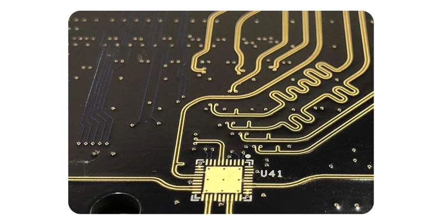
In high-speed digital and RF design, the PCB is no longer just a “carrier” that connects components—it is part of the circuit. When a signal propagates along a PCB trace, it “sees” a transient impedance: the characteristic impedance. A Controlled Impedance PCB is a board where trace geometry (width/spacing), dielectric constant (Dk), and stackup are controlled so that characteristic impedance meets a target (e.g., 50Ω single-ended, 100Ω differential).
Impedance mismatch causes reflections, ringing, and distortion, and can severely impact Signal Integrity (SI)—especially for DDR, PCIe, USB, HDMI and other high-speed interfaces. This FAQ is built around the core keyword what is controlled impedance pcb, and organizes 20 common questions across the full flow—from stackup design to manufacturing delivery—so hardware and PCB teams can execute against a practical baseline.
FAQ overview (20 core questions)
| # | Category | Core question | Key concepts | Quick action |
|---|---|---|---|---|
| 1 | Stackup/Impedance | What is controlled impedance, and why is it required? | Characteristic impedance, reflection | Match source/line/load |
| 2 | Stackup/Impedance | Why does measured impedance differ from simulation? | Dk/Df, etch compensation | Use fab material data + etch factors |
| 3 | Stackup/Impedance | What is Fiber Weave Effect? | Local Dk variation, jitter | Use spread glass, rotate routing |
| 4 | Stackup/Impedance | What happens if a signal crosses a split plane? | Return-path break, EMI | Bridge caps or avoid crossing |
| 5 | Stackup/Impedance | How to choose a reference plane? | GND vs VCC, adjacency | Prefer continuous GND |
| 6 | Layout/Routing | Differential pair fundamentals? | Equal length/spacing, coupling | Maintain symmetry and coupling |
| 7 | Layout/Routing | How tight should length matching be? | Skew | Often < 5 mil; follow datasheet |
| 8 | Layout/Routing | What is a return path? | Minimum-inductance loop | Reference plane adjacent to signal |
| 9 | Layout/Routing | How to optimize high-speed vias? | Via stub, parasitics | Backdrill + GND stitching |
| 10 | Layout/Routing | Serpentine trace: benefits and risks? | Delay tuning, discontinuity | Radius > 3W, spacing > 2W |
| 11 | PI/EMC | How to place decoupling capacitors? | Loop area | Close to pins + via to planes |
| 12 | PI/EMC | Why avoid acute angles? | Acid trap, impedance jump | Use 45° or arcs |
| 13 | PI/EMC | Split ground: good or bad? | Isolation vs return break | Use only when necessary |
| 14 | PI/EMC | How to reduce EMI loop area? | HF current loops | Keep return close to signal |
| 15 | PI/EMC | How to stack power and ground planes? | Plane capacitance, PDN | Tight coupling, ground shielding |
| 16 | Review/Delivery | Why can DRC miss key issues? | Incomplete rules | Build project-based rule templates |
| 17 | Review/Delivery | How to prevent Gerber/BOM/XY mismatch? | Manufacturing errors | Single source + cross-check |
| 18 | Review/Delivery | How to manage ECO effectively? | Version chaos | Formal ECO + version control |
| 19 | Review/Delivery | What is an impedance coupon? | Process verification | Require TDR reports |
| 20 | Review/Delivery | What should DFM review focus on? | Yield & reliability | Pads/vias/spacing/copper limits |
Stackup & impedance
1. Q: What exactly is a controlled impedance PCB, and why must high-speed designs care?
- Symptom: high-speed systems (DDR4, PCIe 4.0) become unstable, eye diagrams fail, or BER increases.
- Root cause: at high frequency, a trace is not an ideal wire—it is a transmission line. If its impedance does not match the source and load, reflections occur. Reflections add to the original waveform, causing overshoot/undershoot and ringing.
- Solution: design stackup and trace geometry (width, dielectric thickness to reference plane, Dk) so characteristic impedance matches the required target (50Ω SE / 100Ω diff).
- Prevention checklist:
- Early in the project, identify all nets requiring impedance control per protocol (USB 3.0, HDMI 2.1, etc.).
- Get accurate Dk/Df values for the chosen materials from your PCB manufacturer.
- Use Polar Si9000 or the impedance calculator in Altium Designer for initial stackup sizing (see our online impedance calculator guide).
- In fab notes, clearly list controlled nets, targets, and tolerances (typically ±10%; critical nets ±5%).
2. Q: Why can my simulated impedance differ significantly from fab TDR coupon results?
- Symptom: you simulate 50Ω, but the fab’s impedance coupon report shows 55Ω—outside ±10%.
- Root cause:
- Material parameter mismatch: generic Dk/Df differs by supplier and lot.
- Unknown process compensation: etching reduces line width (side etch). Good fabs apply etch compensation; if not modeled, final width shrinks and impedance rises.
- Resin content effects: prepreg (PP) flows and fills gaps; final dielectric thickness is often slightly smaller than nominal PP thickness.
- Solution:
- Request the fab’s standard stackup parameters and recommended etch compensation (e.g., HILPCB).
- Provide a detailed stackup drawing with material/thickness targets and require build-to-stackup.
- Prevention checklist:
- Confirm stackup with your fab before design; import parameters into your EDA tool.
- In fab notes, require controlled impedance and attach impedance model screenshots (width/thickness/Dk).
- Require TDR reports for impedance coupons after production.
3. Q: What is Fiber Weave Effect, and how does it affect high-speed signals?
- Symptom: at very high data rates (>10 Gbps), eye jitter is high even with perfect diff-pair length matching.
- Root cause: FR-4 is glass weave + epoxy resin. Glass (Dk ≈ 6) and resin (Dk ≈ 3) differ. If routing runs aligned with glass bundles, effective Dk varies locally; propagation speed shifts slightly and creates timing jitter.
- Solution:
- Use more uniform materials: spread glass (e.g., 1067/1086) reduces local Dk variation.
- Rotate routing angle: rotate critical SerDes channels (e.g., 10–20°) to average weave effects.
- Small zig-zag routing: tiny zig-zags can also average Dk, when used carefully.
- Prevention checklist:
- For 25 Gbps+, prefer high-speed laminates (Megtron 6, Rogers 4350B).
- Plan high-speed bus routing direction; avoid strict alignment to X/Y.
- Ask your fab about weave orientation if needed.
4. Q: What happens when a signal crosses a split reference plane (split plane)?
- Symptom: digital noise couples into sensitive analog circuits, or a high-speed eye collapses.
- Root cause: at high frequency, return current follows the minimum-inductance path directly under (or over) the trace on the reference plane. If a trace crosses a split (e.g., DGND → AGND), the return path is broken and must detour via the nearest connection, creating a large loop:
- Strong EMI radiation: a large loop behaves like an antenna.
- SI degradation: loop inductance increases; impedance discontinuity causes reflections/crosstalk.
- Solution:
- Do not cross: best practice is to re-layout so the signal and its reference plane remain continuous.
- Bridge: if unavoidable, place a high-frequency capacitor (0.1uF or 0.01uF) across the split to provide a return bridge. For diff pairs, provide return bridging for each line.
- Prevention checklist:
- Add design rules forbidding routing across split areas.
- Use EDA SI tools to check return-path continuity.
- Place cross-domain interfaces (e.g., ADC) near the split boundary.
Common pitfall: choosing the reference plane
Not every plane is a good reference plane. Power planes (VCC) can provide a return path, but they are typically noisier and may be discontinuous. Prefer a continuous ground plane adjacent to the signal layer as the main reference. It provides the most stable, lowest-impedance return path and is fundamental for SI.
5. Q: How do I choose the right reference plane for high-speed signals?
- Symptom: the same net looks fine on one layer but degrades sharply after changing layers.
- Root cause: reference-plane quality determines transmission-line performance. An ideal reference plane is:
- Continuous: no large slots/splits.
- Adjacent: close coupling reduces loop area and improves immunity.
- Low-noise: GND is usually “cleaner” than VCC.
- Solution:
- Prefer adjacent ground: for microstrip, reference is the nearest plane below; for stripline, reference is the two planes around it—prefer GND.
- Avoid reference changes: when swapping layers through vias, the reference may change (GND ↔ VCC). Put stitching vias near transitions to connect the two reference planes and keep the return continuous.
- Prevention checklist:
- In stackup design, place high-speed signal layers adjacent to solid ground planes.
- Add DRC rules checking for nearby return stitching vias on layer changes.
- Review PCB stackup tutorial for classic stack structures.
Layout & routing
6. Q: What are the core rules for differential pair routing?
- Symptom: diff links (USB, Ethernet) show weak noise immunity and poor eye opening over distance.
- Root cause: diff-pair advantages (common-mode noise rejection, reduced EMI) rely on symmetry. Anything that breaks symmetry reduces performance.
- Solution: follow three rules: “equal spacing, equal length, common reference”.
- Equal spacing (symmetry): keep pair spacing constant along the entire route to maintain target diff impedance.
- Equal length (timing): tightly match P/N lengths to control skew. Length mismatch converts some differential energy into common-mode.
- Common reference: both lines must reference the same continuous plane so the return paths are symmetric.
- Prevention checklist:
- Define P/N nets as a differential pair and set strict spacing + length rules in the EDA tool.
- Prefer routing the pair on a single layer; minimize vias.
- If layer changes are required, use paired vias and keep the transition symmetric.
7. Q: How tight should differential-pair length matching be?
- Symptom: uncertainty about intra-pair vs inter-pair matching tolerances.
- Root cause: matching depends on bit period. If skew becomes a meaningful fraction of rise time, sampling fails.
- Solution:
- Intra-pair skew (P vs N): very tight. For PCIe Gen3, often < 2 mil; DDR4 clocks/strobes may require < 1 mil. Rule of thumb: keep intra-pair delay below ~20% of the rise-time budget.
- Inter-pair skew: between different pairs (e.g., DDR DQ0 vs DQ1). Usually looser (10–50 mil) depending on timing budget.
- Prevention checklist:
- Read the IC datasheet for the authoritative constraints.
- Use the EDA length-tuning tool (serpentine) for fine compensation.
- Record final lengths and matching deltas in the design report.
8. Q: What is a return path, and why is it so important?
- Symptom: a circuit works at low speed but shows crosstalk/EMI issues as frequency rises.
- Root cause: all current forms a loop. At high frequency, return current follows the minimum-inductance path—directly under the trace on the reference plane.
- Solution:
- Provide continuous reference planes.
- Avoid breaks (splits/slots).
- Keep signal close to reference to reduce loop area.
- Prevention checklist:
- Plan high-speed routing corridors where continuous reference planes exist.
- Use 2D/3D field solvers to visualize return current paths for critical nets.
- Read more: return path design tips.
9. Q: How should I design and optimize vias for high-speed signals?
- Symptom: a well-designed transmission line shows a strong capacitive dip on TDR after a via.
- Root cause: vias are 3D structures with parasitic inductance and capacitance.
- Parasitic capacitance: between via pad and anti-pad.
- Parasitic inductance: along the via barrel.
- Via stub: unused barrel length resonates and can severely attenuate high-frequency content.
- Solution:
- Optimize anti-pad: enlarge anti-pad to reduce capacitance and raise via impedance.
- Add stitching vias: place nearby ground vias to provide a low-inductance return and reduce parasitics.
- Eliminate stubs: for >10 Gbps, use backdrilling or buried/blind vias.
- Prevention checklist:
- Create dedicated via templates for different high-speed signal classes.
- For critical SerDes links, run 3D EM simulation for via transitions.
- In fab notes, mark backdrilled vias and required drill depth clearly.
Need expert support for impedance and stackup design?
Accurate impedance control is a core success factor for high-speed PCB design. If you’re not fully confident in stackup selection, impedance simulation, or via optimization, HILPCB offers professional stackup design and simulation services. Based on your requirements and our manufacturing experience, our engineers can propose optimized stackups and impedance rules—so your design works the first time. Contact us for a free consultation.
10. Q: What does a serpentine trace do, and what risks does it introduce?
- Symptom: you used dense serpentine tuning, but signal quality worsened.
- Root cause: serpentine increases physical length to compensate delay, but poor design causes:
- Impedance discontinuity: bends and adjacent segments couple and change local impedance.
- Coupling/crosstalk: segments too close couple strongly.
- Delay nonlinearity: coupling changes effective propagation speed.
- Solution:
- Bend radius: R ≥ 3W.
- Segment spacing: S ≥ 2W (more for very fast nets and diff pairs).
- Limit tuned length per segment and distribute tuning.
- Prevention checklist:
- Configure serpentine rules in EDA to enforce spacing and radius.
- Avoid placing serpentine immediately at endpoints of diff pairs.
- Prefer global layout optimization; use serpentine only for final fine-tuning.
Power Integrity & EMC
11. Q: How should decoupling capacitors be placed for maximum effectiveness?
- Symptom: high-speed ICs behave unstably; supply rails show noise and logic levels jitter.
- Root cause: fast switching draws transient current. Decoupling provides a local low-impedance charge reservoir. Poor placement increases loop inductance and weakens decoupling.
- Solution: minimize loop area from capacitor to IC pins.
- Close to pins (VCC/GND).
- Prefer via-to-plane: short trace into a via, then into planes.
- Use multiple values (0.1µF + 0.01µF + 100pF) to cover bandwidth; smallest caps closest.
- Prevention checklist:
- Follow reference designs from the IC vendor.
- Plan the decoupling network at schematic time.
- Place critical decaps first in layout.
12. Q: Why should PCB routing avoid acute angles (< 90°)?
- Symptom: after fabrication, corners show over-etch or copper residue.
- Root cause:
- Manufacturing (Acid Trap): etchant accumulates in inner corners causing over-etch; outer corners may under-etch.
- SI: sharp corners create an impedance step and reflections (critical in RF).
- Solution:
- Use 45° corners (common and safe).
- Use arcs (best for RF / ultra-high speed).
- Prevention checklist:
- Set the EDA default corner style to 45° or arcs.
- Add DRC rules to detect acute angles.
13. Q: Is split ground good or bad—should I use it?
- Symptom: you split DGND and AGND to isolate noise, but analog noise got worse.
- Root cause: splitting can break return paths. Any trace crossing the split creates a large EMI loop and couples noise system-wide.
- Solution:
- Modern best practice: prefer a single solid ground plane with good placement zoning.
- Use split ground only in special cases (high-precision ADC/DAC reference, strict safety isolation), with single-point connection and no crossing traces.
- Prevention checklist:
- Default to a solid ground plane for new projects.
- If splitting is required, perform strict “cross-split” checks.
- Learn more: ground plane best practices.
14. Q: How do I reduce EMI radiation loop area effectively?
- Symptom: EMC test fails; radiated emissions are over limits.
- Root cause: larger high-frequency current loop area radiates more effectively.
- Solution:
- Ensure tight return paths with continuous reference planes.
- Optimize decoupling to shrink transient current loops.
- Keep strong radiators (clocks, switch nodes) short and away from board edge.
- Add shielding: stripline structures, and via fences around edges where appropriate.
- Prevention checklist:
- Identify major noise sources and sensitive zones early.
- Use EMC rule checking to flag large loops.
15. Q: How should power and ground planes be stacked?
- Symptom: uncertainty about best plane order in a multilayer board.
- Root cause: stacking affects plane capacitance, EMI shielding, and PDN impedance.
- Solution:
- Tight coupling: adjacent power + ground forms large plane capacitance, lowering HF PDN impedance.
- Ground as shield: place GND on outer/near-outer layers to shield internal signal layers.
- Power-plane pullback: shrink power plane by ~20H relative to ground to reduce edge radiation (H = plane separation).
- Prevention checklist:
- Example 6-layer stack: Signal – GND – Signal – Signal – Power – GND.
- Avoid adjacent signal layers without an intervening ground plane.
Review & delivery
16. Q: Why can DRC show “No Violations” but the board still has issues?
- Symptom: DRC passes, but fabricated boards have shorts/opens or performance problems.
- Root cause: DRC only checks the rules you define. Incomplete rules make DRC ineffective.
- Solution:
- Build a complete rule set: beyond spacing/width, include length matching, via limits, diff-pair rules, cross-split checks, silkscreen-to-pad clearance, etc.
- Sync rules with the PCB fab’s process capability.
- Use experienced manual review for critical paths, PDN, and grounding.
- Prevention checklist:
- Maintain separate DRC templates for high-speed, RF, and power projects.
- After DRC, run a detailed pcb design checklists.
17. Q: How do I prevent inconsistency between Gerber, BOM, and pick-and-place (XY) files?
- Symptom: assembler reports footprint mismatch or incorrect XY placement/orientation.
- Root cause: outputs are generated independently; manual edits introduce mismatches.
- Solution:
- Use a single source of truth: generate all outputs from the final locked design database.
- Use batch tools/automation to export consistently.
- Cross-check: load Gerbers and XY in a viewer and spot-check against BOM.
- Prevention checklist:
- Standardize file naming and versioning.
- Include an assembly drawing with designators, orientation, and outlines.
18. Q: How do I manage ECO effectively?
- Symptom: multiple schematic/PCB changes cause version chaos and wrong builds.
- Root cause: no formal change control; unclear records and poor team sync.
- Solution:
- Implement an ECO flow: request → review → impact analysis → approval → execution.
- Use version control (Git/SVN) with clear change notes.
- Sync documents: schematic, PCB, BOM, design notes, and bump version/date.
- Prevention checklist:
- Define ECO owners at project start.
- Stamp version/date into filenames and within documents for every release.
19. Q: What is an impedance coupon, and why is it important?
- Symptom: you see “odd test patterns” on panel rails.
- Root cause: those are impedance coupons (test coupons). They replicate the same geometry/layer of controlled lines and allow fab verification by TDR.
- Solution:
- Require coupons for all controlled lines and request TDR reports from manufacturers like HILPCB.
- Verify measured impedance falls within your tolerance (e.g., 100Ω ±10%); request analysis or rebuild on out-of-spec.
- Prevention checklist:
- In fab notes, list layers, widths, targets, and tolerances for all controlled nets.
- Make the TDR report a mandatory incoming QC document.
20. Q: What should DFM review focus on?
- Symptom: functional design is fine, but the fab says it’s not manufacturable or yield will be low.
- Root cause: design exceeds process capability (min features, drill limits, assembly constraints).
- Solution: DFM review ensures manufacturability, testability, and assembly. Focus on:
- Base process limits: min width/spacing, min drill, annular ring, copper-to-edge.
- Via strategy: avoid via-in-pad unless you use via fill/plugging.
- SMT/DIP: spacing for soldering/rework; readable silkscreen; proper solder mask.
- Panelization: V-cut / mouse-bite design and process rails.
- Prevention checklist:
- Request the fab’s DFM guide before design.
- Use EDA DFM checks for early screening.
- Send design files for professional DFM review before release.
DFM & delivery checklist
| Area | Check item | Requirement | Owner |
|---|---|---|---|
| Schematic | Library consistency | All parts from validated central library | Designer |
| ERC | No floating pins / power conflicts | Designer | |
| BOM completeness | Full refdes/PN/footprint/description | Designer | |
| Stackup/Impedance | Stackup confirmation | Material/thickness/Dk/Df confirmed with fab | Design/Process |
| Impedance rules | All controlled nets have correct rules | Designer | |
| Plane continuity | No splits/large voids under HS nets | Designer | |
| Placement | Modular placement | Digital/analog/power/RF clearly separated | Designer |
| Critical placement | Decaps, crystals, connectors optimized | Designer | |
| Thermal | Heatsources have copper/vias/space | Designer | |
| Manufacturable spacing | Component-to-component/edge spacing OK | Designer | |
| Routing | Power nets | Short and wide power, solid ground | Designer |
| High-speed | Diff pairs/clocks follow constraints | Designer | |
| Length match | All length matching met and recorded | Designer | |
| Via optimization | GND stitching, no stub risk on key nets | Designer | |
| Acute angles/copper islands | No acute corners; no floating copper | Designer | |
| Silk/Assembly | Silkscreen clarity | Refdes visible; orientation clear | Designer |
| Polarity | Clear polarity markers for diodes/caps/ICs | Designer | |
| Fiducials | ≥3 fiducials, L-shape distribution | Designer | |
| Production files | Gerbers | Correct layer order, RS-274X | Designer |
| Drill files | Size/plating correct, aligned to Gerbers | Designer | |
| BOM | Matches schematic + PCB | Designer | |
| XY | Origin/unit/rotation correct | Designer | |
| Fab notes | Material, thickness, impedance, finish, etc. | Designer | |
| Final review | DFM review | Fab or senior engineer final check | Process/External |
| Version control | All outputs from locked release | Designer |
Recommended learning path
Mastering controlled impedance PCB design is a continuous journey. Here’s a suggested path from fundamentals to advanced practice:
- Beginner (core concepts)
- Book: Signal Integrity Simplified by Eric Bogatin.
- Articles: official blogs from Altium, Cadence, etc. (stackup basics, differential pair basics).
- Intermediate (practical execution)
- Book: High-Speed Digital Design: A Handbook of Black Magic by Howard Johnson.
- Standards: IPC-2152 (conductor sizing) and IPC-2221 (general PCB design).
- Tools: impedance calculators, length tuning, 3D field analysis.
- Advanced (simulation mastery)
- Software: SI/PI tools such as Ansys SIwave, Keysight ADS, Simbeor.
- Training: SI/PI/EMC professional courses.
- Community: participate in forums (e.g., aihpcb.com) and exchange with experts.
From design to manufacturing: HILPCB supports your success
Understanding “what is controlled impedance pcb” is only the first step. Applying theory in real designs is the real challenge. HILPCB is not only a high-quality PCB manufacturer, but also a technical partner. We provide:
- Free DFM review: identify manufacturing risks before release.
- Professional stackup and impedance services: tailored stackup rules balancing performance and cost.
- Reliable impedance control and testing: each controlled impedance lot can include accurate TDR reports.
Ready for your next high-speed PCB project? Contact our technical team for a quote and free design consultation.
Conclusion
This FAQ organized 20 common questions around what is controlled impedance pcb with practical answers, prevention checklists, DFM focus points, and learning resources—helping teams build an executable design baseline and reduce risk across stackup, routing, and manufacturing delivery. If you follow the checklists and involve HILPCB’s DFM/DFA team early, you can speed up prototype-to-production while maintaining quality and compliance.
For fabrication and assembly support, contact HILPCB Turnkey Assembly or SMT Assembly for DFM/DFT guidance.
Common Questions
What is a controlled impedance PCB?
It is a PCB where trace geometry, dielectric properties, and stackup are controlled so the signal sees a target characteristic impedance.
Why does controlled impedance matter in real products?
It reduces reflections, ringing, and distortion on high-speed or RF signals, improving signal integrity and link stability.
Why can measured impedance differ from simulation?
Differences in fab process, actual material properties, copper etch effects, and stackup variation can all shift final impedance.
What should teams control first to get reliable results?
They should align stackup, reference planes, routing rules, and fabrication capability early, then verify with DFM and test feedback.