
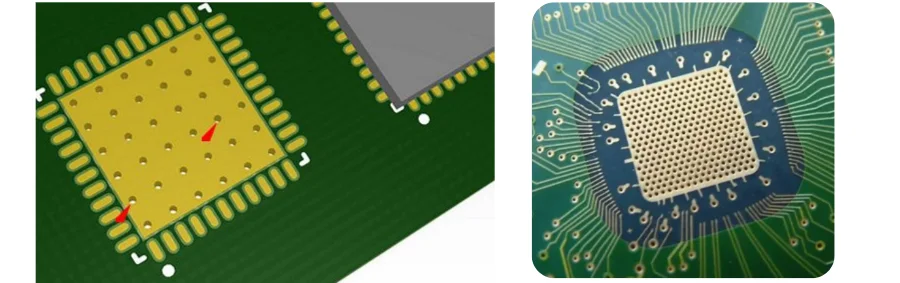
In today’s data-driven era—from data centers and AI accelerators to 5G/6G infrastructure—bandwidth and throughput demands are growing exponentially. 112G, 224G, and even higher-rate SerDes links are becoming the norm, creating unprecedented challenges for PCB design. Engineers must meet stringent Signal Integrity (SI) requirements while also dealing with the massive heat generated by high-performance silicon. In this context, Copper coin (embedded copper block) stands out as a key solution for balancing ultra-high-speed signal transmission with efficient thermal management. It is not merely a heatsink element—it is a foundation for keeping the entire system stable and reliable.
As an engineer experienced in TDR/VNA measurements and S-parameter analysis, I know how every dB of loss and every ps of jitter can make or break a link. Traditional approaches such as thermal via arrays are no longer sufficient when facing FPGA, ASIC, and GPU devices at 150W and beyond. This article breaks down Copper coin in depth—from fundamentals, to impacts on SI and Power Integrity (PI), to interaction with advanced stack-up design, and finally the key manufacturing controls—so you can tackle the dual challenges of high-speed PCB design with confidence.
What is Copper coin, and what are its core advantages?
Copper coin is an advanced manufacturing process where a pre-machined solid copper block (typically high-purity C1100 copper) is embedded into a pre-made cavity or through-feature in the PCB. The copper block directly contacts the thermal pad of the heat source (e.g., a BGA-packaged chip) and extends through the board to the opposite side, where it can interface with a large heatsink or a chassis cold plate—creating a very low thermal-resistance heat path.
Its core advantages include:
Outstanding thermal conductivity: Copper’s thermal conductivity is about 400 W/m·K, far higher than FR-4 (~0.25 W/m·K) and higher than the effective thermal conductivity of plated vias. With solid Copper coin, heat is transferred quickly and efficiently from the die hotspot—often tens of times more effective than thermal via arrays. This is critical to keep the chip in its optimal temperature range and prevent Hot Spot-driven throttling or damage.
Improved Power Integrity (PI): The embedded copper block is often tied to GND. Because it is large and solid metal, it provides an ultra-low-inductance, low-impedance return path for high-current flow. This reduces PDN impedance and suppresses Ground Bounce and SSN, while giving nearby high-speed signals a stable, clean reference plane.
Better mechanical strength and stiffness: A heavy copper block significantly increases local stiffness under the BGA region. This helps reduce stress from CTE mismatch during shock, vibration, or thermal cycling, improving long-term BGA solder-joint reliability.
Design flexibility: The shape, size, and thickness of Copper coin can be customized for different packages and thermal needs. It can be T-shaped, I-shaped, or otherwise contoured to optimize heat flow and mechanical interfacing.
How does Copper coin solve thermal challenges in high-speed design?
In high-speed digital systems, signal attenuation is closely related to temperature. As chip temperature rises, not only does the silicon performance degrade, it also heats the surrounding PCB dielectric, shifting dielectric constant (Dk) and loss factor (Df). This impacts transmission-line Controlled impedance and attenuation—ultimately degrading SI.
Copper coin addresses this head-on by building a “thermal highway”:
- Direct contact and efficient conduction: The chip’s Thermal Pad is coupled to the smooth Copper coin surface via TIM or direct soldering. Heat flows from the junction into the copper block with minimal barrier.
- Lateral and vertical spreading: Beyond strong Z-axis conduction, the copper block’s mass provides excellent lateral spreading (X-Y plane), distributing concentrated hotspots into a broader area and lowering local temperature rise.
- Seamless external heat removal: The opposite end of the copper block is typically flush with (or slightly protruding from) the PCB backside, enabling direct contact to large heatsinks, liquid cold plates, or chassis. Compared with indirect conduction through FR-4 and multiple vias, metal-to-metal contact dramatically reduces interface thermal resistance.
For very high-current applications such as high-power supply modules, designs may also use Heavy copper 3oz+ PCB processes. Copper coin can be integrated seamlessly with thick copper layers to form a robust electro-thermal management system that carries hundreds of amps while efficiently removing Joule heat.
Thermal solution performance comparison
| Attribute | Copper Coin | Thermal via array (Thermal Vias) | Embedded vapor chamber (Vapor Chamber) |
|---|---|---|---|
| Effective thermal conductivity | Very high (≈400 W/m·K) | Low to medium (50-150 W/m·K) | Extremely high (1500-2000+ W/m·K) |
| Thermal resistance | Very low | Relatively high | Very low |
| Impact on signal routing | Large routing keep-out | Can route between vias, but constrained | Very large routing keep-out |
| Manufacturing cost | High | Low | Very high |
| Best-fit scenarios | High-power ASIC/FPGA, optical modules | Medium/low-power devices, QFN packages | Server CPU/GPU with extreme thermal demands |
Copper coin’s double-edged impact on SI: opportunities and risks
From a SI perspective, Copper coin is a double-edged sword. Used correctly, it improves system performance; ignored, it can cause catastrophic link failure.
Opportunities (positive impacts):
- Stable reference plane: As noted above, a GND-connected copper block provides an extremely stable “zero potential” reference. This is especially important for differential pairs because both traces see a consistent reference environment—maintaining accurate Controlled impedance and reducing common-mode conversion.
- Lower crosstalk: The copper block acts as a large ground structure that helps isolate signals across regions. For example, it can physically separate noisy power circuits from sensitive SerDes lanes, reducing EMI and crosstalk.
- Temperature stability: By keeping the chip and nearby region cooler, Copper coin helps maintain stable Dk/Df in PCB materials (e.g., Rogers PCB) during operation. This stability is critical for long-reach, high-data-rate links—because even small Dk/Df drift can drive impedance mismatch and higher loss.
Challenges (negative impacts):
- Reference-plane discontinuity: If a high-speed net crosses the edge of Copper coin, it encounters a reference-plane break/split. Return current is forced to detour, creating a large loop area, which can drive strong reflections, radiation, and EMI issues.
- Impedance discontinuity: Even if a trace routes on a signal layer above the block, the reference beneath changes from a thin copper foil plane to a thick copper mass. Geometry and field distribution shift dramatically, often lowering impedance abruptly—creating a capacitive discontinuity and reflections.
- Routing channel blockage: The copper block consumes valuable PCB real estate and creates a large keep-out below and around it, making BGA fan-out in dense regions much more challenging.
To overcome these, plan early: strictly prohibit high-speed routing across the block edge; place dense ground Stitching Vias around the block to maintain return-path continuity; use 3D EM simulation to model the coupling impact to adjacent transmission lines, and tune line width/spacing to compensate for impedance shifts.
Copper coin interaction with advanced PCB stack-up design
Successful Copper coin implementation relies on tight integration with advanced stack-up design—especially in complex systems that combine high-speed signals and high-power devices. A single material or structure rarely satisfies all constraints.
This is where Hybrid stack-up (Rogers+FR-4) shows unique value. The strategy uses low-loss, high-performance materials (e.g., Rogers, Megtron series) on outer layers or stripline layers for critical high-speed signals, while using lower-cost FR-4 for power/ground planes or low-speed layers.
Integrating Copper coin into a Hybrid stack-up (Rogers+FR-4) can balance performance and cost:
- Maximize performance: Route 56G/112G+ differential pairs on Rogers layers to minimize insertion loss and dispersion, while Copper coin removes heat directly from top-side ASIC/FPGA devices for stable operation.
- Control cost: Use expensive low-loss materials only where needed, reducing overall PCB cost.
- Design integration: In stack-up planning, precisely define block thickness, embed depth, and the relationship to each layer. For example, the top of the block must achieve excellent Co-planarity with outer copper to ensure reliable BGA soldering.
In dense BGA regions around the block, Via-in-Pad plated over (VIPPO) is also critical. VIPPO builds vias directly in BGA pads, then fills with conductive resin and plates over to create a flat pad surface. This shortens routing, reduces parasitic L/C, and is key to high-density fan-out and high-speed performance. The organic combination of Copper coin, Hybrid stack-up (Rogers+FR-4), and Via-in-Pad plated over (VIPPO) forms the “three-horse carriage” of modern high-performance high-speed PCB design.
🔥 Copper Coin design & thermal-management key points
Define Copper Coin geometry and embed depth early in placement. Treat it as a key Mechanical Constraint, and ensure precise alignment to the power-device Thermal Pad.
Do not route high-speed signals across physical gaps between the copper block and reference plane. Place Stitch Vias at the edge to maintain a continuous return-impedance path and avoid excessive EMI radiation.
Use high-thermal-conductivity TIM between the package and the block. Tightly control Bondline Thickness (BLT) to minimize total contact thermal resistance and fully realize copper’s conductivity.
Communicate deeply with Highleap PCB Factory. Pre-assess risks around Coin Coplanarity, adhesive overflow after pressing, and CTE mismatch across different materials.
Copper pillar vs. Copper coin: how to choose
When discussing internal metal thermal structures, Copper pillar is another commonly mentioned technique. Although both use copper’s strong thermal conductivity, it differs from Copper coin in structure, use cases, and process.
Definition and structure:
- Copper coin: A standalone, pre-machined solid copper block embedded into the PCB via press-fit and/or bonding. It is typically large, covering most or all of the package footprint.
- Copper pillar: Copper columns typically “grown” by PCB plating, with smaller diameters and often arranged in dense arrays. They may be solid columns or copper-filled vias.
Primary applications:
- Copper coin: Focuses on “point” thermal removal for a single high-power device—macro-scale heat transport.
- Copper pillar: Focuses on fine-grained thermal management and electrical interconnect. It is often used in HDI boards or IC substrates as conductive/thermal vertical paths, or as micro thermal pillars under a chip.
Selection guidance:
- For a large BGA with TDP > 100W, Copper coin is the clear first choice.
- For multiple distributed lower-power devices (e.g., QFN power ICs), or extremely crowded regions requiring both vertical interconnect and heat conduction, Copper pillar arrays can be more advantageous.
- In some designs, the two can be combined: a large Copper coin handles the main heat flow, while Copper pillar handles local hotspots elsewhere.
Copper coin is “heavy artillery” for core thermal challenges; Copper pillar is “precision-guided” for fine and distributed electro-thermal needs.
Key manufacturing steps and quality control for Copper coin PCB
Embedding a large metal block into a precision multilayer PCB is a highly challenging manufacturing task. Success depends directly on process precision and quality control. As a factory focused on advanced PCB manufacturing, Highleap PCB Factory (HILPCB) has accumulated deep experience in Copper coin processes.
Key steps include:
- Cavity routing: Use high-precision CNC equipment to mill a cavity matching the block geometry into a partially laminated stack. Depth control is critical and directly impacts final coplanarity.
- Copper block fabrication and surface treatment: The block must be machined to micron-level tolerances, and the surface may require treatment (e.g., ENIG) to ensure reliable bonding to inner layers and later soldering.
- Press-fit & bonding: Place the block into the cavity. Depending on design, use pure interference press-fit and/or fill/fix with high-thermal-conductivity adhesive. Temperature and pressure must be tightly controlled to avoid damaging the PCB base material.
- Planarization: After pressing, small height differences can remain between the block and surrounding PCB. Grinding/polishing is used to achieve the required surface roughness and coplanarity for BGA soldering (typically within ±1 mil).
- Subsequent lamination and plating: After embedding, proceed with outer-layer lamination, drilling, and plating. Chemistry and temperatures must be controlled to avoid degrading the bond interface between the copper block and dielectric.
Quality control runs through the entire process. HILPCB uses X-Ray inspection to verify internal connectivity and void-free interfaces, cross-section analysis to validate bond quality, and high-precision profilometry to measure final coplanarity. For designs involving Heavy copper 3oz+, we maintain dedicated etching and plating lines to ensure thick-copper pattern accuracy and uniformity.
HILPCB advanced process capability
| Process parameter | HILPCB capability | Why it matters for Copper Coin design |
|---|---|---|
| Max layer count | 64 layers | Supports complex high-speed backplanes and server mainboards |
| Copper thickness range | 0.5oz - 20oz | Fully supports Heavy copper 3oz+ and thicker copper designs |
| Impedance control accuracy | ±5% | Ensures reliable Controlled impedance for high-speed channels |
| Minimum mechanical drill | 0.15mm | Supports high-density interconnect and fine Via-in-Pad structures |
| Surface coplanarity control | ±0.025mm (1 mil) | Ensures soldering reliability for BGA and high-frequency connectors |
How to accurately predict Copper coin performance via simulation
Given Copper coin’s strong impact on thermal/electrical performance and its higher manufacturing cost, accurate multi-physics simulation before building hardware is essential. It validates the design, finds risks early, and avoids expensive re-spins.
Simulation is typically done in two dimensions:
Thermal simulation:
- Goal: predict junction temperature under workload, PCB temperature distribution, and heat-flow paths.
- Tools: Ansys Icepak, Flotherm, SimScale, etc.
- Key inputs: accurate 3D models (stack-up, Copper coin, package, TIM, heatsink, etc.), material thermal properties (k, specific heat), power dissipation, and environment (airflow, ambient).
- Outputs and analysis: confirm whether Copper coin cooling meets requirements, optimize block geometry, and decide whether stronger external cooling is needed.
Electromagnetic simulation:
- Goal: evaluate Copper coin impact on SI and PI.
- Tools: Ansys HFSS, CST Microwave Studio, Keysight ADS, etc.
- SI analysis: extract S-parameters of transmission lines that include the Copper coin structure, analyzing insertion loss, return loss, and crosstalk. Pay special attention to nets that pass near the block edge to confirm performance does not degrade sharply—critical to maintaining accurate Controlled impedance.
- PI analysis: analyze PDN impedance vs. frequency to verify that Copper coin as a low-impedance ground path suppresses noise in targeted bands.
Successful simulation follows “Garbage In, Garbage Out.” Accurate material parameters, detailed geometry, and simulation settings aligned with real manufacturing processes are prerequisites for trustworthy results. HILPCB’s engineering team can provide DFM review, combining our tolerance and material databases with your simulation models to maximize correlation to the final physical product.
Application outlook: Copper coin in future data centers and AI hardware
Looking ahead, as Moore’s Law evolves and heterogeneous computing accelerates, chip integration and power density will continue rising. Single-chip power at 300W or even 500W will become common. Under this trend, Copper coin will become more widely used and more critical.
- Next-gen data centers: In 224G+ SerDes channels, budgets for loss and jitter are extremely tight. By stabilizing chip temperature, Copper coin indirectly keeps low-loss materials such as Hybrid stack-up (Rogers+FR-4) consistent—supporting long-reach (LR) backplanes and optical-module interconnects.
- AI and HPC accelerators: GPUs and dedicated AI chips are power-hungry. Copper coin is among the most effective PCB-level cooling approaches, enabling compute cores to sustain top frequency and deliver full performance.
- Co-Packaged Optics (CPO): CPO co-packages optical engines and switch silicon on the same substrate, reducing electrical path length but greatly increasing heat flux density. Copper coin and similar embedded thermal structures are core to CPO substrate design.
- Automotive electronics: With electrification and intelligence, the cooling demands of high-power IGBT modules, LiDAR, and domain controllers keep rising. Robust, efficient Copper coin techniques have strong potential in these high-reliability fields as well.
Combined with high-density routing processes like Via-in-Pad plated over (VIPPO), Copper coin will support next-generation packages with more pins and tighter pitch—pushing the performance boundary of the electronics industry.
Conclusion
Copper coin is not just an advanced cooling method—it is a system-level solution that reshapes high-speed PCB design. It bridges thermal management, SI, and PI, and is a must-have tool for engineers chasing extreme performance. From tight Controlled impedance control, to balancing cost/performance with Hybrid stack-up (Rogers+FR-4), to achieving high density with Via-in-Pad plated over (VIPPO), successful Copper coin adoption reflects the complexity and system nature of modern PCB design.
At the same time, this powerful technique places very high demands on manufacturing. Choosing a partner like Highleap PCB Factory (HILPCB) with deep expertise and advanced equipment is critical. We can not only build Heavy copper PCB to your strict requirements, but also provide end-to-end services from design review and simulation support to turnkey PCBA assembly, ensuring your innovation lands perfectly.
If you are developing next-generation high-performance products and facing difficult thermal and SI challenges, contact our technical experts today. Let’s explore how Copper coin can help your product achieve a powerful yet cool “core”.