
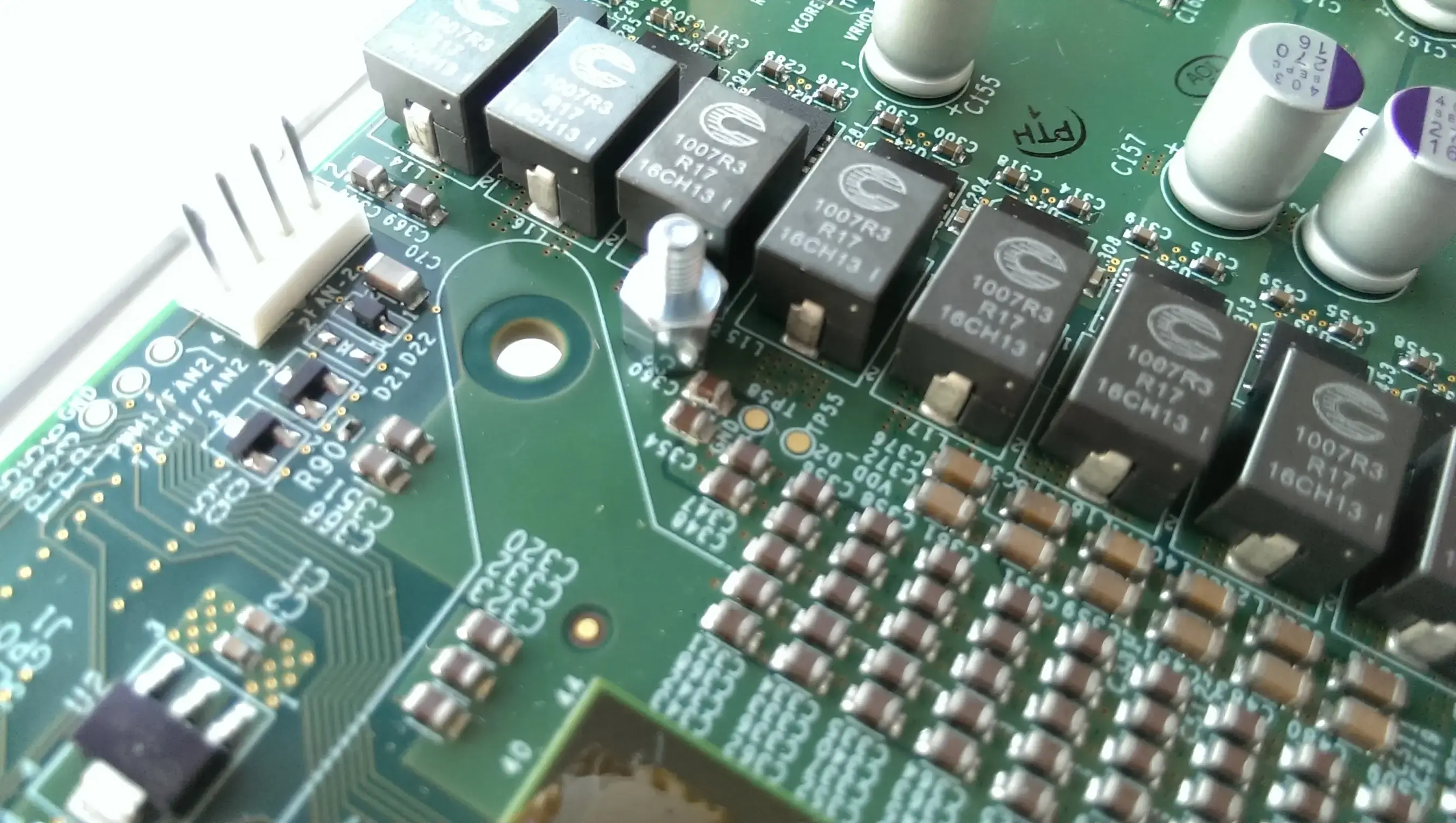
A cryptocurrency PCB is a board used in high-power mining hardware, blockchain node infrastructure, secure key-management equipment, or crypto-enabled retail payment devices. The design challenge is not “crypto” by itself; it is the combination of high-current power delivery, dense compute routing, thermal control, secure hardware partitioning, and reliable manufacturing.
For OEM teams, the right review starts by separating three different board routes. A mining hash board is usually dominated by ASIC power delivery and airflow. A blockchain node or exchange server board is dominated by high-speed interconnect and storage/network reliability. A hardware wallet, HSM, or crypto payment terminal is dominated by tamper awareness, secure element integration, RF/payment interfaces, and compliance-boundary documentation.
Key Takeaways
- Cryptocurrency PCB design should be reviewed by application route, not by the word “cryptocurrency” alone.
- Mining hash boards need strong PDN design, thermal paths, connector current capacity, and repeatable assembly more than generic “high-speed” wording.
- Blockchain node servers and payment-gateway hardware may require high-speed PCB planning for PCIe, Ethernet, DDR, storage, and accelerator interfaces.
- HSM PCB and wallet hardware can support secure elements, tamper loops, enclosure sensors, and controlled routing, but the PCB alone does not prove FIPS, PCI PIN, PCI PTS, or payment-system certification.
- Contactless payment and crypto retail terminals add RF antenna layout, shielding, display/keypad interfaces, battery management, and field-service reliability concerns.
- A useful RFQ should include power maps, thermal targets, security boundary drawings, stackup needs, inspection requirements, and functional-test expectations.
In This Guide
- What is a cryptocurrency PCB?
- Cryptocurrency PCB, HSM PCB, and payment terminal PCB are not the same route
- Mining hash board design: power, heat, and ASIC chain reliability
- High-speed design for blockchain nodes and payment gateway hardware
- Power integrity and thermal control for 24/7 operation
- Security boundaries for HSM, wallet, and payment hardware
- HDI, BGA, inspection, and assembly controls
- Common failure modes
- Cost drivers
- RFQ checklist
- Why work with HILPCB
- Reference standards and specifications
- FAQ
What is a cryptocurrency PCB?
A cryptocurrency PCB is not one fixed board type. In real projects, the phrase can point to several different hardware families: ASIC mining hash boards, GPU or accelerator carrier boards, blockchain node servers, hardware wallet boards, HSM boards, crypto ATM modules, or retail payment terminals that support digital-asset workflows. Each family stresses the PCB in a different way.
The biggest mistake is to treat one board technology as if it solves every crypto-related product. Mining boards are usually power-and-thermal problems. Server boards are interconnect-and-validation problems. HSM boards are secure-hardware and tamper-boundary problems. Retail terminals are RF, power, UI, environmental, and payment-interface problems. The review becomes clearer when those routes are separated early.
| Board route | Typical hardware | Dominant PCB burden | What the PCB can support | What the PCB alone cannot prove |
|---|---|---|---|---|
| Mining hash board | ASIC chains, controller MCU, fans, temperature sensors, high-current input | PDN, copper weight, thermal vias, connector current, airflow serviceability | Stable high-current distribution and repeatable assembly | Mining profitability, hashrate, or energy ROI |
| Blockchain node/server board | CPU, DDR, PCIe, SSD/NVMe, Ethernet, accelerators | Stackup, controlled impedance, via stubs, PDN, thermal zones | High-speed signal and power integrity planning | Network throughput or protocol performance without system validation |
| HSM PCB | Secure processor, secure element, battery-backed memory, tamper sensors | Secure partitioning, tamper loop routing, shielding, controlled test access | Physical support for key-protection architecture | FIPS 140-3, PCI HSM, or PCI PIN approval by itself |
| Hardware wallet PCB | Secure MCU/SE, display, buttons, USB/BLE/NFC, battery | Low-power design, secure routing, enclosure sensors, production test | Secure element integration and tamper-aware layout | Wallet security claims without firmware, enclosure, audit, and device testing |
| Crypto retail/POS terminal | Contactless reader, keypad, display, printer/scanner options, network module | RF antenna layout, power domains, ESD, connector durability, battery/charging | Payment-interface and security hardware integration | PCI PTS, EMV, or payment-network approval by itself |
A buyer looking for a mining hash board needs different data than a buyer building an HSM module. A single quote form that asks only for Gerbers and quantity will miss important risks: current peaks, copper thickness, RF antenna clearance, security boundary, BGA inspection, firmware programming, and end-of-line test requirements.
Cryptocurrency PCB, HSM PCB, and payment terminal PCB are not the same route
The phrase Cryptocurrency PCB attracts several adjacent keywords: HSM PCB, Contactless Payment PCB, Magnetic Stripe PCB, Laser Scanner PCB, and Impact Printer PCB. Those terms can belong in one digital-finance ecosystem, but they should not be merged into one board claim.
An HSM PCB is a security-focused board. It may include secure processors, battery-backed memory, tamper meshes, enclosure switches, encrypted management interfaces, and controlled service ports. Its PCB layout should support security objectives by reducing exposed attack surfaces, separating sensitive nets, controlling test access, and documenting tamper-boundary assumptions. But actual HSM approval depends on the cryptographic module, firmware, enclosure, key management, physical security requirements, validation lab process, and operational procedures.
A contactless payment PCB is a payment-terminal interface board. It may include an NFC/contactless antenna, secure element or secure processor, display/keypad interfaces, battery charging, USB, wireless, SAM slots, and point-of-sale communications. The board must respect RF antenna geometry, ground clearance, ESD paths, and user-facing connector durability. But it does not become a payment-approved terminal simply because the PCB hosts a contactless antenna or secure chip.
A mining board is usually closer to a power electronics and thermal-management problem. The core questions are whether ASIC power rails are stable, current is shared safely, heat can leave the package, connectors are rated with enough margin, temperature sensors are placed meaningfully, and the first build can be tested under realistic airflow. This route should not borrow HSM or payment-terminal security language unless the product really contains a secure payment function.
A retail commerce control board may contain more modest electronics: a magnetic stripe reader, barcode or laser scanner interface, impact printer driver, coin acceptor, card dispenser, keypad, display, or network module. These boards share reliability and ESD concerns with crypto payment terminals, but their design center is usually field serviceability and transaction uptime rather than high-density mining compute.
A practical rule is to use the application name to explain the board context, then describe the actual PCB burden. That produces clearer copy and better manufacturing intake.
Mining hash board design: power, heat, and ASIC chain reliability
A mining hash board is usually a high-current, thermally stressed assembly built around repeated ASIC devices. Even when the digital signaling is not as complex as a datacenter server motherboard, the board can still fail quickly if the power path, thermal path, and mechanical support are weak.
The PDN is the first review item. Mining ASICs often operate at low core voltages with very high current demand. That pushes the PCB toward wide copper pours, short current loops, low-resistance planes, well-placed bulk and high-frequency decoupling, and careful separation between noisy switching loops and sensitive clock/control circuits. For higher-current areas, heavy copper PCB construction may be appropriate, but copper weight should be chosen with the actual current map, temperature rise target, and manufacturability constraints in view.
The second review item is current entry. Board-edge power connectors, bus bars, screw terminals, or blade connectors must be evaluated together with copper spreading and heat rise. A connector that looks acceptable on current rating alone may still run hot when airflow is blocked, contact resistance increases, or multiple boards are packed tightly in a chassis.
The third review item is ASIC-chain routing. Many hash boards arrange ASICs in repeated chains. Clock, reset, data, and control lines need stable reference paths, consistent routing, and enough margin against power-switching noise. A single weak solder joint, cracked via, or marginal connector can cause a whole chain to disappear during production test.
The fourth review item is temperature measurement. Temperature sensors should be placed where they represent actual thermal risk. A sensor too far from the ASIC hotspot may report acceptable values while package or solder-joint temperatures are already stressing the assembly. Thermal simulation, board bring-up, and infrared inspection can help correlate sensor location with the real heat path.
| Mining hash board area | Design concern | PCB/PCBA control | Evidence to request |
|---|---|---|---|
| ASIC power rail | High current and low voltage margin | Heavy copper, short loops, decoupling, VRM placement | Power map, current estimate, thermal target |
| Power input | Connector heating and voltage drop | Connector footprint review, copper spreading, torque/strain relief | Connector datasheet, input-current profile |
| ASIC chain routing | Chain instability or intermittent devices | Reference continuity, clean clock/reset routing, test pads | Netlist, chain test plan |
| Thermal path | Hotspots, throttling, solder fatigue | Thermal vias, copper pours, heatsink interface planning | Thermal model or prototype temperature data |
| Fan/control interface | Cooling loss or false tach reading | ESD protection, connector retention, current margin | Fan spec, control logic, fault response plan |
| Production test | Marginal chain pass/fail ambiguity | ICT/FCT pads, boundary access where possible | Hash-board functional test criteria |
High-speed design for blockchain nodes and payment gateway hardware
Blockchain node servers, exchange infrastructure, payment gateways, and HSM appliances often look more like server and networking hardware than mining boards. Their board risk moves toward high-speed interfaces, storage reliability, secure management ports, and repeatable validation.
PCIe, Ethernet, DDR, USB, NVMe, and management interfaces are not marketing labels. They create concrete PCB obligations: stackup planning, controlled impedance, reference-plane continuity, connector launch design, via-stub control, differential-pair spacing, and insertion-loss budgeting. A design using PCIe 5.0, for example, should be treated as a high-speed interconnect project with strict route classification and validation planning rather than a generic multilayer PCB.
Low-loss material selection should be driven by channel length, speed, connector count, and loss budget. Not every cryptocurrency or retail-commerce board needs premium laminate. A compact hardware wallet may not need the same material class as a payment gateway server. A high-speed accelerator card or node server may require a hybrid stackup, smoother copper, tighter dielectric control, or backdrilling. The right route is the one that matches the channel, not the one that sounds most advanced.
| Interface or subsystem | Common PCB risk | Practical control |
|---|---|---|
| PCIe/NVMe storage | Insertion loss, reflections, via stubs | Controlled stackup, backdrill where justified, connector launch review |
| DDR memory | timing skew, reference noise, dense escape routing | length matching, stable reference planes, PDN planning, simulation handoff |
| Ethernet/SFP/QSFP | connector transition loss, EMI, cage grounding | launch tuning, chassis-ground strategy, shielding and test planning |
| USB/service ports | ESD, shield grounding, mechanical stress | TVS placement, connector retention, ground reference continuity |
| Secure management port | unintended debug access or service exposure | controlled test access, secure boot support, production lock plan |
| Payment gateway processor | power transients and heat | staged PDN review, thermal via arrays, BGA X-ray inspection |
For HILPCB intake, high-speed projects should include the target interfaces, lane rates, impedance requirements, stackup proposal, connector models, insertion-loss sensitivity, and whether the customer expects TDR coupons, impedance reports, X-ray inspection, or functional test support.
Power integrity and thermal control for 24/7 operation
Cryptocurrency and digital-finance hardware often runs continuously. That does not mean the PCB must promise uptime by itself. It means the board should be designed so the system has a realistic path to uptime: clean rails, controlled heat rise, robust solder joints, adequate current margin, and predictable field-service behavior.
Power integrity starts with the current path. VRMs, inductors, MOSFETs, bulk capacitors, BGA processors, ASICs, and connectors must be reviewed as one power network. Wide copper is helpful, but plane transitions, via count, connector heating, capacitor placement, and return current path can be just as important. In a dense board, a small layout shortcut around a VRM can become a repeatable heat or noise problem.
Thermal control starts with a heat map. ASICs, GPUs, FPGAs, network processors, power switches, and laser/scanner drivers create different thermal profiles. Some need local heat spreading under the package. Some need airflow channels. Some need thermal vias under exposed pads. Some need the mechanical team to define heatsink pressure, TIM thickness, and service access. A PCB quote that excludes thermal assumptions will rarely catch these issues early.
| Thermal or PI decision | What to review | Typical manufacturing impact |
|---|---|---|
| Copper weight | Current, heat spreading, etch tolerance | Heavier copper improves current capacity but affects trace precision and cost |
| Layer count | PDN impedance, routing density, shielding | More layers improve routing and reference planes but increase lamination complexity |
| Thermal vias | Heat transfer from packages to planes/heatsinks | Via fill, solder wicking, and pad design must match assembly process |
| VRM placement | transient response and loop area | Layout affects EMI, heat, and voltage droop |
| Decoupling strategy | rail stability across frequency | BOM, placement, and BGA escape routing must be coordinated |
| High-Tg material | temperature margin and dimensional stability | Useful for sustained heat, but not a substitute for real thermal design |
| Conformal coating | moisture and contamination protection | Coating can affect rework, connector masking, and thermal behavior |
For mining systems, thermal failure is often visible as throttling, chain dropout, solder fatigue, connector discoloration, or intermittent boot behavior. For HSM and payment hardware, thermal drift may appear as random resets, sensor false alarms, clock instability, RF detuning, or premature battery aging. In both cases, the board should be reviewed with the enclosure and airflow assumptions included.
Security boundaries for HSM, wallet, and payment hardware
Security-sensitive cryptocurrency hardware deserves careful wording. A PCB can support secure design, but it cannot single-handedly prove cryptographic security, payment approval, or tamper resistance. Those claims require system-level hardware, firmware, enclosure, lifecycle, testing, and certification evidence.
For HSM PCB work, the board may support secure processors, cryptographic accelerators, battery-backed memory, secure clocking, tamper mesh layers, enclosure switches, anti-probing routing, and controlled service interfaces. PCB layout matters because exposed traces, uncontrolled debug headers, weak battery backup, or poor shielding can undermine the security model. But validation against cryptographic-module or payment-industry requirements belongs to the complete module and its documented operating environment.
For hardware wallet PCB work, the board may include a secure element, display, buttons, USB-C, BLE, NFC, battery charging, and seed-entry controls. The PCB should minimize opportunities for probing sensitive nets, separate user-interface circuits from secure key paths, and document which interfaces are locked during production. Still, the final security depends on firmware, boot chain, key storage, user interface, enclosure design, update process, and audit.
For contactless payment or crypto POS terminals, the PCB adds RF and payment-interface risks. Antenna geometry, ground keepout, matching network accessibility, ESD entry path, battery noise, display noise, and keypad/display flex routing can all affect payment-terminal behavior. But EMV, PCI PTS, PCI PIN, or payment network approval is not a PCB-level claim.
| Security-related feature | PCB-level support | Certification boundary |
|---|---|---|
| Secure element / secure MCU | Power integrity, routing, shield planning, controlled test access | Device security still depends on firmware, key management, and validation |
| Tamper loop or mesh | Layer planning, continuity routing, connector/enclosure interface | Tamper resistance must be tested in the full enclosure and threat model |
| Battery-backed domain | isolated low-leakage routing, retention supply, test access | Key retention and zeroization behavior are system-level functions |
| Debug/service port | access control pads, production lock plan, documentation | Secure lifecycle control must include firmware and manufacturing process |
| NFC/contactless interface | antenna keepout, matching, EMI/ESD control | Payment/contactless approval requires device-level testing |
| HSM appliance interface | shielded management ports, grounding, controlled assembly | FIPS/PCI HSM approval belongs to a complete cryptographic module or device |
A good RFQ for security-sensitive work should include a security-boundary drawing, debug-lock requirements, masking or no-probe zones, battery-backed sections, secure-element package details, enclosure assumptions, and production programming needs. Without those details, the PCB supplier can only quote the board mechanically, not support the security intent.
HDI, BGA, inspection, and assembly controls
High-density cryptocurrency, HSM, and payment-terminal boards often require close coordination between PCB fabrication and assembly. The risk is not only trace width or layer count. The real question is whether the manufacturing flow can reproduce the design intent across SMT, inspection, programming, and functional test.
HDI can help route fine-pitch BGAs, secure processors, compact RF/payment modules, and dense power-management circuits. Blind vias, buried vias, microvias, and via-in-pad structures should be justified by routing density, package pitch, and signal integrity. Overusing HDI increases cost and yield pressure; underusing it can force compromised escapes and weak reference paths.
For BGA and QFN devices, inspection planning is essential. AOI cannot see hidden solder joints. X-ray inspection is often needed for BGA solder bridges, voiding, head-in-pillow, and alignment. For secure devices, inspection may also need to preserve tamper or coating boundaries. If conformal coating or potting is planned, inspection and functional test should occur before irreversible protection steps whenever possible.
| Process step | What it catches or controls | Why it matters |
|---|---|---|
| DFM/DFA review | spacing, annular ring, via-in-pad, stencil concerns, connector access | prevents production risk before the first build |
| Stackup review | impedance, PDN, copper balance, warpage | protects high-speed and power behavior |
| SPI | solder paste volume and alignment | catches print defects before placement |
| AOI | polarity, missing parts, visible solder defects | supports fast feedback on SMT quality |
| X-ray | BGA/QFN hidden joints, voids, bridges | critical for dense compute and secure processor packages |
| ICT or flying probe | opens, shorts, passive values, basic nets | catches assembly and fabrication defects early |
| Boundary-scan/JTAG | digital connectivity where physical probing is limited | useful for BGA-heavy boards if designed in |
| Functional test | rails, boot, communication, sensor/RF checks | confirms the board behaves in its intended subsystem |
| Programming/serialization | firmware, keys/config placeholders, device ID | links the board to traceability and customer records |
For turnkey assembly projects, it is better to define these controls at quotation stage. Waiting until boards arrive at assembly to ask for X-ray, serialization, functional test, or selective conformal coating can create delays and rework.
Common failure modes in cryptocurrency and digital-finance PCBs
| Failure mode | Likely root cause | How to reduce risk before release |
|---|---|---|
| ASIC chain dropout | marginal solder joint, unstable clock/reset, weak connector, rail droop | X-ray where relevant, power-rail margin, chain test access, connector review |
| Burned power connector | underestimated current, poor contact resistance, airflow obstruction | connector derating, thermal rise test, copper spreading, mechanical strain relief |
| Random server reset | PDN noise, BGA voiding, thermal hotspot, memory/PCIe instability | PDN review, BGA inspection, thermal validation, high-speed test plan |
| Contactless payment read failure | antenna detuning, ground intrusion, display/battery noise, poor ESD path | antenna keepout, matching access, ESD placement, enclosure correlation |
| HSM tamper false alarm | noisy tamper line, weak pull state, battery-domain instability | shielded routing, clean retention supply, environmental test, secure test plan |
| Firmware mismatch | poor serialization or programming control | MES traceability, firmware version lock, production traveler |
| Field corrosion | inadequate coating, residue, condensation, connector exposure | cleaning control, coating mask plan, humidity/salt exposure validation |
| BGA intermittent fault | head-in-pillow, voiding, thermal-cycle fatigue | stencil review, reflow profile control, X-ray inspection, thermal cycling plan |
| EMI failure | large switching loops, poor shield transition, noisy cable entry | layout review, filter placement, chassis-ground plan, pre-compliance test |
| Debug exposure | unsecured test pads or service headers | production lock process, documented no-access areas, lifecycle control |
Cost drivers
Cryptocurrency and secure retail hardware costs are not driven by board size alone. The expensive items are usually stackup complexity, copper weight, high-current connectors, fine-pitch packages, inspection requirements, security-related handling, and functional-test fixtures.
| Cost driver | Why it increases cost | When it is worth it |
|---|---|---|
| Heavy copper | harder etching and plating control | high-current mining boards, VRM-heavy power sections |
| High-speed material | laminate cost and process sensitivity | long PCIe/Ethernet/DDR channels with tight loss budgets |
| HDI / via-in-pad | sequential lamination and via fill | fine-pitch secure processors, compact terminals, dense BGA escape |
| Backdrilling | extra drilling and registration control | high-speed server or gateway boards with through-via stubs |
| X-ray inspection | equipment time and inspection documentation | BGA/QFN-heavy assemblies and high-reliability hardware |
| Conformal coating | masking, curing, inspection, rework complexity | humid retail, outdoor, industrial, or corrosive environments |
| Functional test fixture | fixture design and software effort | production programs where boot, RF, sensor, or power validation matters |
| Serialization/MES | data capture and traveler control | HSM, payment, field-service, warranty, or batch-traceable programs |
The cheapest build is rarely the best first build for a security-sensitive or high-current board. A slightly more complete prototype package can reveal PDN, thermal, antenna, or inspection issues before they become expensive field problems.
RFQ checklist for cryptocurrency, HSM, and retail payment PCBs
Send more than Gerbers when requesting a quote. The files below help HILPCB return useful DFM and assembly feedback instead of only a price.
Board data
- Gerber or ODB++ files
- IPC-356 netlist if available
- Drill files and stackup request
- Finished copper weight and surface finish requirements
- Controlled-impedance requirements and coupon expectations
- Panelization constraints if the board fits a rack, chassis, or terminal enclosure
Power and thermal data
- ASIC/GPU/processor power map
- rail voltages and current estimates
- VRM placement intent
- connector current and cable-entry assumptions
- heatsink, TIM, airflow, fan, or enclosure constraints
- expected continuous-duty environment
High-speed and RF data
- PCIe, Ethernet, DDR, USB, NFC, or wireless interface list
- connector models and target lane rates
- antenna keepout, matching network location, and enclosure material
- backdrill or via-stub constraints
- requested impedance tolerance or simulation notes
Security and payment data
- secure-element or secure-MCU package details
- tamper-loop or tamper-mesh boundary drawing
- battery-backed domain requirements
- debug/service-port lock requirements
- serialization, firmware programming, or unique-ID process
- payment-terminal or HSM compliance targets as system context only
Assembly and test data
- BOM with approved alternates
- centroid / pick-and-place file
- assembly drawings
- X-ray, AOI, ICT, flying probe, or functional-test expectations
- conformal coating or potting areas and keepout zones
- packaging, ESD, labeling, and traceability requirements
Why work with HILPCB
HILPCB supports cryptocurrency, secure hardware, and retail-commerce electronics as board-level engineering problems rather than buzzword categories. The practical value is in matching the manufacturing route to the dominant risk: high-current mining, high-speed server interconnect, secure hardware partitioning, or contactless payment interface integration.
For high-current boards, HILPCB can review copper weight, connector geometry, thermal vias, heavy copper feasibility, and assembly constraints. For server and gateway boards, we can support controlled-impedance stackups, high-speed material selection, BGA inspection planning, and high-speed PCB manufacturing review. For compact secure devices or terminals, we can support HDI PCB construction, fine-pitch assembly, X-ray inspection, conformal coating planning, and turnkey assembly coordination.
The most useful engagement point is before layout is frozen. Send the stackup, power map, connector plan, security boundary, and test requirements early. That gives the engineering team enough context to catch manufacturability, thermal, inspection, and test-access risks before they are buried under first-build schedule pressure.
Reference standards and specifications
These references are listed as technical context only. They should not be read as PCB-level compliance claims.
- PCI Express Base Specification, PCI-SIG
- PCI PIN Security Standard, PCI Security Standards Council
- PCI PTS POI Security Requirements, PCI Security Standards Council
- PCI PTS HSM Security Requirements, PCI Security Standards Council
- FIPS 140-3, NIST
- ISO/IEC 19790
- ISO/IEC 14443
- EMV Contactless Specifications, EMVCo
- IPC-A-600
- IPC-A-610
- IPC-6012
- IPC-2221
- IPC-7095
- J-STD-001
FAQ
Is a cryptocurrency PCB the same as a mining hash board?
No. A mining hash board is one cryptocurrency PCB route, usually dominated by ASIC power delivery, thermal design, and chain reliability. Cryptocurrency PCB can also refer to blockchain server boards, HSM boards, hardware wallets, crypto ATM modules, or payment-terminal hardware.
Does a mining PCB improve hashrate or profitability by itself?
Not by itself. The PCB can reduce power loss, improve thermal stability, support cleaner rails, and improve production consistency, but hashrate and profitability also depend on ASIC selection, firmware, cooling system, power cost, pool conditions, maintenance, and market conditions.
Can a PCB be FIPS 140-3 or PCI certified?
A bare PCB normally cannot prove those approvals by itself. The PCB can support a cryptographic module, HSM, or payment terminal architecture, but FIPS 140-3, PCI HSM, PCI PIN, or PCI PTS evaluation is performed at the module or device level with hardware, firmware, enclosure, lifecycle, and operating procedures included.
What makes HSM PCB layout different from ordinary server PCB layout?
An HSM PCB may require secure-element routing, tamper-loop continuity, battery-backed domains, shielding, controlled debug access, and traceability. These items support the security model, while the actual security claim still depends on the complete cryptographic module and validation process.
When should a cryptocurrency or payment hardware board use HDI?
Use HDI when package pitch, board size, secure routing, RF layout, or connector density cannot be solved cleanly with conventional through-hole via routing. HDI should be justified by design constraints because it increases manufacturing complexity and cost.
What should I send for a cryptocurrency PCB quote?
Send Gerbers or ODB++, BOM, stackup, current map, thermal targets, controlled-impedance requirements, connector details, security boundary drawings, antenna keepout, assembly drawings, and inspection or functional-test requirements.
Next steps
If your project involves a mining hash board, HSM module, crypto retail terminal, or high-speed blockchain infrastructure board, start the manufacturing review before layout is locked. The costliest problems are usually hidden in current entry, BGA escape, thermal path, debug exposure, RF keepout, and production test access.
Send your Gerber or ODB++ package, BOM, power map, stackup target, security boundary, and assembly-test requirements to [email protected], or upload them through the Quote page. HILPCB can review the package for high-current routing, high-speed stackup risk, HDI feasibility, BGA inspection needs, conformal coating, and turnkey PCBA handoff.