
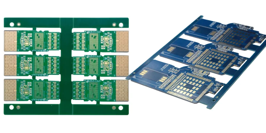
With the explosive growth of AI, machine learning, and cloud computing, data-center traffic is rising at an unprecedented rate. Traditional “pluggable” optical-module architectures are approaching physical limits in power, density, and signal integrity. In this context, Co-packaged Optics (CPO) emerged: it co-packages the optical engine and the switch ASIC on the same substrate to attack the I/O bottleneck at the root. But this disruptive architecture also brings unprecedented PCB design and manufacturing challenges. To successfully manage electro-optical co-design, thermal/power constraints, and precision assembly complexity, you must perform a comprehensive DFM/DFT/DFA review at project kickoff. It’s not only a design-optimization tool—it is a strategic core for smooth transitions from prototype to mass production and for overall commercial success.
Why DFM/DFT/DFA review is central in CPO design
In traditional PCB flows, DFM (Design for Manufacturability), DFT (Design for Testability), and DFA (Design for Assembly) are often treated as separate, late-stage check steps. In CPO, that fragmented model fails. CPO is system-level electro-optical co-design—any missed detail can sink the entire program. Therefore, an integrated DFM/DFT/DFA review must span the full product lifecycle, especially across NPI EVT/DVT/PVT phases.
- DFM (manufacturability): Can the PCB/substrate be built with high yield and acceptable cost? For CPO this includes ultra-fine geometry, tight impedance control, low-CTE materials, and complex hybrid lamination.
- DFA (assemblability): How to assemble optical engines, ASICs, fiber arrays, etc. efficiently and reliably on the substrate—alignment tolerances, curing processes, heatsink installation, and connector layout.
- DFT (testability): How to test the product during manufacturing and in the field. CPO test is complex: you must validate high-speed electrical performance (e.g., PAM4 eye/BER) and optical-link behavior. DFT ensures enough test access and built-in mechanisms.
Bringing these into a single early review helps you foresee and remove manufacturing/assembly/test bottlenecks at the concept stage—shortening development cycles and reducing risk throughout NPI EVT/DVT/PVT.
Electro-optical interconnect: high-speed signal and optical-path co-existence from a DFM perspective
The core CPO idea is shortening high-speed electrical paths as much as possible—but that requires harmony between electrical routing and optical paths in micrometer-scale space. The goal of the DFM review here is to ensure the design is physically manufacturable without sacrificing performance.
High-speed electrical-interconnect challenges: CPO modules often carry 100Gbps-per-lane or higher PAM4 signals, pushing SI to extremes. DFM review focuses on:
- Material selection and stack-up: Choose ultra-low-loss high-speed PCB materials and coordinate them with the interposer/substrate stack so impedance remains continuous from ASIC to optical engine.
- RDL to board-level routing: From chip Redistribution Layer (RDL) to PCB traces, every segment geometry and via structure (e.g., back-drilling) must be validated via EM simulation and DFM analysis to control loss and reflections.
- Tolerance control: Line width/spacing and dielectric thickness tolerances directly affect impedance. DFM rules must be set based on real manufacturing capability (e.g., HILPCB), not idealized simulation assumptions.
Precision optical interface design: Aligning the Fiber Array to the optical engine is one of the most critical CPO assembly steps—often requiring ±1μm accuracy.
- Datums and alignment marks: DFA review ensures clear, high-precision Fiducial Marks on the PCB for automated optical alignment (AOI) positioning.
- V-groove and mechanical structures: Tolerance and position accuracy of the V-groove base that carries fibers directly affects coupling efficiency. DFM ensures these structures can be manufactured and integrated with high precision.
- Verification mechanisms: Alignment verification must be planned in the design stage. A rigorous First Article Inspection (FAI) report validates DFM/DFA results by comparing design intent to first-build measurements—confirming all key dimensions and tolerances are under control.
Table 1: CPO vs. traditional optical-module PCB design parameters
| Parameter | Traditional pluggable module PCB | CPO substrate/PCB |
|---|---|---|
| Data rate per lane | 25G / 50G NRZ/PAM4 | 100G / 200G PAM4 |
| Material requirements | Mid/low-loss FR-4 or equivalent | Ultra-low-loss materials, low-CTE substrates, ceramics |
| Impedance tolerance | ±10% | ±5% ~ ±7% |
| Assembly alignment accuracy | ~ ±25μm (electrical connectors) | ~ ±1μm (optical interface) |
| Thermal management | Module-level cooling, power < 15W | System-level co-thermal design, power > 100W |
Thermal-management challenge: power distribution and heat-flow paths from a DFA perspective
CPO places a hundreds-of-watts ASIC right next to temperature-sensitive optical engines, creating a massive thermal challenge. Poor thermal design hurts performance and can cause permanent damage. DFA review ensures the cooling solution is not only effective, but also can be assembled precisely and reliably in real production.
Power distribution and hotspot analysis:
- Thermal budget: Early in design, define the power and max operating temperature of each component (ASIC, optical engine, driver IC) and build a detailed thermal budget.
- Co-simulation: Use CFD to model the entire module, locate hotspots, and evaluate different cooling solutions.
Assembly-ready thermal structure design:
- Heatsink / Vapor Chamber: DFA review checks fixing methods, flatness requirements of the contact surface, and whether installation pressure on delicate components is controllable.
- TIM: Selecting TIM and defining a robust application process is critical. DFA assesses thickness control and the risk of TIM overflow contaminating optical surfaces.
- Heat-flow optimization: Design Thermal Vias and Copper Coin structures in a high-thermal PCB to conduct heat efficiently from silicon to heatsink. DFA ensures these features don’t conflict with high-speed signal vias.
- Encapsulation and protection: Some designs use Potting/encapsulation to protect fragile optics. Potting thermal conductivity and CTE must be evaluated strictly to avoid becoming a thermal barrier or adding thermal stress.
Materials and stack-up: DFM-driven reliability and warpage control
Materials are the foundation of a CPO substrate. Large CTE mismatches between silicon photonics, organic interposers, and the main PCB are a root cause of package warpage and long-term reliability problems.
Selecting and applying low-CTE materials:
- Core materials: DFM review guides selection of substrate materials with CTE closer to silicon, such as Rogers PCB materials and other low-CTE hydrocarbon/ceramic-filled laminates—critical for thermal-stress control.
- Hybrid stack-up: To balance cost and performance, designs often use hybrid lamination: expensive low-CTE high-speed materials on outer layers with more conventional materials in the core. DFM review must ensure compatibility and reliable lamination processes.
How DFM controls warpage:
- Symmetry: Keeping the stack-up (dielectrics and copper distribution) symmetric is the simplest and most effective warpage-control method.
- Copper balance: DFM tools analyze copper coverage per layer and add non-functional copper pour to balance stress and reduce bow/twist.
- Process impact assessment: Thermal shocks from reflow, wave soldering, or THT/through-hole soldering for specific connectors can introduce stress. DFM review estimates these impacts and applies design compensation early.
CPO substrate DFM implementation flow
- Step 1: early co-design - Align with a manufacturer like HILPCB in the concept stage to obtain key inputs such as material properties and process capability.
- Step 2: define materials and stack-up - Select low-CTE materials and a symmetric hybrid stack-up based on thermal/electrical performance and reliability targets.
- Step 3: simulation-driven iteration - Run SI/PI and thermo-mechanical co-simulations and iterate layout/routing accordingly.
- Step 4: comprehensive DFM/DFA/DFT review - Use professional tools and checklists to validate design rules, tolerances, assembly, and test requirements.
- Step 5: prototype build and FAI - Build first prototypes and execute strict First Article Inspection (FAI) to compare measured data against design targets.
- Step 6: production introduction - Finalize optimizations and lock the fabrication/assembly flow for volume production.
Assembly and integration: key DFA considerations
CPO assembly is a complex fusion of semiconductor packaging, SMT, and precision optical assembly. DFA review’s goal is to make this process efficient, repeatable, and reliable.
Precision assembly process design:
- Fiber alignment and fixation: DFA defines jig design for stable support without obstructing alignment tools, and precisely specifies epoxy dispense volume and curing profiles (UV or thermal) to avoid stress-induced misalignment.
- Mixed-technology soldering: CPO substrates often include SMT parts and may also include through-hole connectors requiring higher mechanical strength. DFA evaluates Selective wave soldering feasibility to protect nearby heat-sensitive parts. By contrast, traditional THT/through-hole soldering may require stricter local thermal shielding.
- Protective encapsulation: Potting/encapsulation is key to protecting fiber interfaces and delicate optics from moisture, dust, and mechanical shock. DFA review optimizes potting-zone design to ensure complete fill without bubbles and defines clear processes for consistency across NPI EVT/DVT/PVT.
As a provider of one-stop PCBA services, HILPCB understands the importance of DFA in complex products and can deliver end-to-end optimization advice from PCB fabrication to precision assembly.
Testability design: DFT ensures CPO performance and reliability
“If you can’t test it, you can’t manufacture it.” For highly integrated CPO products, DFT is especially critical. Once packaged, many internal nodes become physically inaccessible.
DFT strategies and execution:
- Built-in test circuits: Integrate BIST and Loopback in ASICs and driver ICs to validate high-speed links without relying solely on expensive external equipment.
- Test pads and probing: DFT review requires high-frequency probe pads on critical signal paths for production measurements (eye diagram and BER) with scopes and BER testers. Pad design must support high-frequency probing.
- In-system monitoring interfaces: Designs must comply with industry standards such as CMIS and provide I2C access for real-time monitoring of temperature, power, optical power, and other parameters.
- FAI as the final DFT validation: First Article Inspection (FAI) is not only dimensional validation; it verifies DFT effectiveness by confirming probe access and expected signals—ensuring smooth production testing.
DFT key reminders
- Plan early: Define the test strategy in architecture design—not after layout completion.
- Layered testing: Build a layered approach from wafer → die → module → system to filter defects step by step.
- Automation first: Design for automated testing to reduce manual intervention and improve efficiency and consistency.
- Traceable data: Record and trace test data for every module to enable yield analytics and process improvement.
How HILPCB empowers your CPO program with comprehensive DFM/DFT/DFA review
In the CPO frontier, choosing a partner that understands both design intent and manufacturing reality is crucial. HILPCB is not just a PCB manufacturer—we empower product success with DFM/DFT/DFA review across the program.
Our strengths include:
- Advanced process capability: Ultra-low-loss materials, ±5% impedance control, and high-precision IC substrates for robust manufacturing foundations.
- Expert engineering support: Engineers who understand CPO’s unique electrical, optical, thermal, and mechanical requirements, delivering early optimization guidance.
- Flexible assembly options: From prototypes to volume, including mixed-soldering technologies like Selective wave soldering and precision Potting/encapsulation processes.
- Strict quality control: Full First Article Inspection (FAI) and advanced test equipment to meet the harshest performance and reliability requirements.
Conclusion
Co-packaged Optics (CPO) is pushing data-center interconnect into a new era. But realizing its potential requires a systematic, forward-looking design-and-manufacturing methodology. Comprehensive DFM/DFT/DFA review is the core of that methodology: it embeds manufacturability, testability, and assemblability into every design detail, solving electro-optical co-design, thermal management, material matching, and precision assembly challenges at the root. By working closely with an experienced partner like HILPCB and executing rigorous reviews and optimizations early, you can reduce risk, accelerate time-to-market, and win in the next-generation data-center race.
Common Questions
Why is DFM/DFT/DFA review critical for data-center optical modules and CPO programs?
CPO and optical module products combine optical alignment, high-speed electrical channels, thermal density, and fine assembly tolerances in one system. A full review is what keeps those coupled risks under control before they become yield or reliability problems.
Why must electro-optical co-design and thermal management be reviewed together?
Signal performance, optical path stability, and heat flow all interact in compact optical modules. If any one of those areas is optimized without the others, the final product can become difficult to assemble or unstable in real service.
Why is testability so important in advanced optical interconnect products?
These products require more than basic continuity checks because hidden defects can exist in optical coupling, high-speed channels, or precision assembly interfaces. A strong DFT plan is essential for catching those issues before shipment.
Why should teams involve a capable manufacturing partner early in CPO development?
Experienced partners can guide materials, stackup, precision assembly flow, and production test strategy while there is still room to adapt the design. That early feedback significantly reduces program risk and schedule loss.