
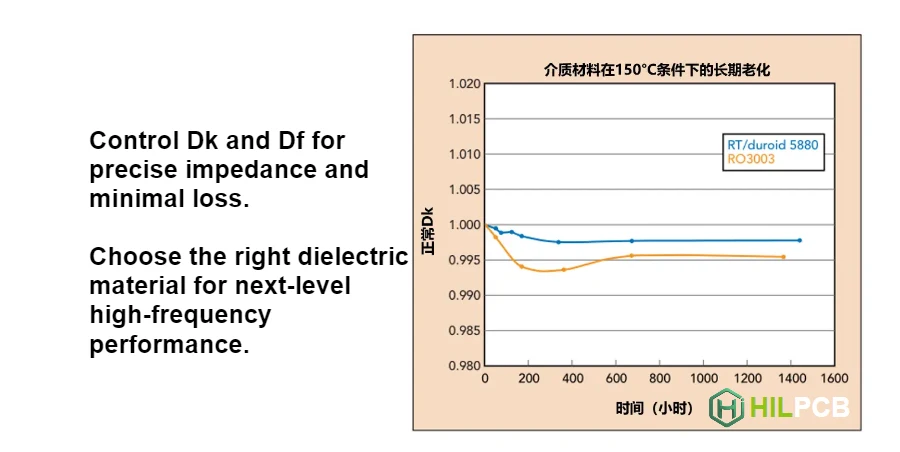
The dielectric constant (Dk, relative permittivity $\varepsilon_r$) is the fundamental material property that governs electromagnetic wave propagation speed, characteristic trace impedance, and signal delay across printed circuit board laminates. Understanding how the dielectric constant interacts with the dissipation factor (Df) is critical for RF, microwave, and high-speed digital hardware design.
This guide provides comprehensive understanding of dielectric properties and their practical implications for high frequency PCB material performance.
HILPCB provides detailed material data and engineering support to help customers select materials with optimal dielectric properties for their RF and microwave applications.
What Is Dielectric Constant? Definition, Units and Formula
The dielectric constant (commonly denoted as Dk in PCB engineering, or relative permittivity $\varepsilon_r$ in electrodynamics) is the ratio of the electrostatic capacitance of a capacitor using the dielectric material ($C$) to the capacitance of an identical capacitor in a vacuum ($C_0$):
$$\varepsilon_r = \frac{C}{C_0} = \frac{\varepsilon}{\varepsilon_0}$$
- Unit: Dimensionless (unitless, 1). Because it is a ratio of two identical physical quantities (absolute permittivity $\varepsilon$ over vacuum permittivity $\varepsilon_0 \approx 8.854 \times 10^{-12} \text{ F/m}$), dielectric constant has no dimensional units.
- Signal Propagation Velocity Formula: In TEM propagation (such as a balanced stripline transmission line), electromagnetic wave velocity $v$ is inversely proportional to the square root of the dielectric constant: $$v = \frac{c}{\sqrt{\varepsilon_r}} \approx \frac{2.998 \times 10^8 \text{ m/s}}{\sqrt{\varepsilon_r}}$$ In imperial engineering units, the propagation delay $\tau_d$ is calculated as: $$\tau_d \approx 84.72 \cdot \sqrt{\varepsilon_r} \text{ [ps/inch]}$$
- Relationship with Dissipation Factor (Df): While Dk determines the capacitive energy storage and phase velocity of the dielectric, Df (dissipation factor, loss tangent $\tan\delta$) determines the dielectric attenuation (signal loss converted to heat). The dielectric attenuation per unit length ($\alpha_d$) is directly proportional to frequency, $\sqrt{\varepsilon_r}$, and $\tan\delta$: $$\alpha_d \approx 2.3 \cdot f \cdot \sqrt{\varepsilon_r} \cdot \tan\delta \text{ [dB/inch (f in GHz)]}$$
Typical PCB Substrate Dielectric Constant (Dk) Comparison
| PCB Material Class | Typical Substrate Example | Dielectric Constant (Dk @ 10 GHz) | Loss Tangent (Df @ 10 GHz) | Recommended Application |
|---|---|---|---|---|
| Standard Epoxy FR-4 | Shengyi S1000-2 / Isola 370HR | 4.2 – 4.5 | 0.015 – 0.020 | General purpose, low-speed digital (< 1 GHz) |
| Hydrocarbon Ceramic | Rogers RO4350B | 3.48 ± 0.05 | 0.0037 | RF power amps, cellular base stations, 5G |
| Hydrocarbon Ceramic | Rogers RO4003C | 3.55 ± 0.05 | 0.0027 | Automotive radar, satellite LNB, high-speed digital |
| PTFE / Woven Glass | Rogers RT/duroid 5880 | 2.20 ± 0.02 | 0.0009 | Millimeter-wave, aerospace radar (up to 77 GHz) |
| Polyimide (Flex PCB) | DuPont Pyralux AP | 3.40 | 0.0020 | Flexible interconnects, aerospace high-temp |
Dielectric Constant Fundamentals
Dielectric constant (Dk, also called relative permittivity εr) measures how much a material concentrates electric fields compared to vacuum. It fundamentally affects signal propagation and circuit dimensions.
At HILPCB, we verify material Dk through controlled impedance testing, ensuring actual performance matches design expectations.
Physical Meaning
Dk indicates how easily the material polarizes in response to an electric field. Higher Dk means stronger polarization, which:
- Increases capacitance between conductors
- Slows electromagnetic wave propagation
- Shortens effective wavelength in the material
- Reduces characteristic impedance for given geometry
Impact on Impedance
Characteristic impedance depends on Dk through the geometry-material relationship:
For microstrip: Z₀ decreases as Dk increases (approximately inversely with √Dk)
Practical implication: Higher Dk materials require narrower traces for the same impedance target. A 50Ω trace might be 15 mils wide in FR-4 (Dk4.3) but only 8 mils wide in a Dk10 ceramic material.
Impact on Propagation
Signal velocity in the material:
v = c / √Dk (approximately, for stripline)
Lower Dk means faster propagation. PTFE (Dk2.2) propagates signals ~40% faster than FR-4 (Dk4.3).
Impact on Wavelength
Wavelength in the material shortens by √Dk:
λ_material = λ_freespace / √Dk
This affects distributed element sizing. A quarter-wave section at 10 GHz in PTFE is physically longer than in FR-4.
Dissipation Factor and Loss
Dissipation factor (Df, also called loss tangent or tan δ) quantifies how much electromagnetic energy the dielectric absorbs and converts to heat. Lower Df means less signal attenuation.
HILPCB offers materials across the full Df range, from standard FR-4 to ultra-low-loss PTFE laminates for demanding applications.
Physical Mechanism
When an alternating electric field passes through the dielectric, molecular dipoles try to align with the field. Energy is lost through:
- Dipole rotation friction
- Ionic conduction
- Electronic polarization losses
These losses increase with frequency in most materials.
Loss Contribution
Dielectric loss per unit length:
α_dielectric ∝ f × Df × √Dk
Key insight: Dielectric loss increases linearly with frequency. At high frequencies, this becomes the dominant loss mechanism, making Df the critical parameter.
Dielectric Property Ranges by Material Class
Practical Loss Example
Comparing materials at 10 GHz, 6-inch 50Ω microstrip:
- Standard FR-4 (Df=0.020): ~6 dB loss
- Low-loss FR-4 (Df=0.008): ~2.5 dB loss
- Rogers RO4350B (Df=0.004): ~1.3 dB loss
- PTFE (Df=0.001): ~0.4 dB loss
Material choice dramatically affects achievable performance.
Frequency Dependence of Dielectric Properties
Both Dk and Df vary with frequency—a critical consideration for wideband designs.
Understanding frequency behavior: Frequency Response of PCB Material
Dk Frequency Dependence
Most materials show decreasing Dk with increasing frequency:
- FR-4: Dk may drop from 4.5 at 1 MHz to 4.0 at 10 GHz
- PTFE: Very stable, typically <2% variation across frequency
- Ceramic-filled: Good stability, ~3-5% variation
This variation affects impedance consistency across frequency and causes dispersion (different frequencies travel at different speeds).
Df Frequency Dependence
Df behavior varies by material type:
- FR-4: Df increases moderately with frequency
- Low-loss materials: Df relatively stable
- PTFE: Df may decrease slightly at higher frequencies
Dispersion Effects
When Dk varies with frequency, different spectral components of a signal travel at different speeds, causing pulse spreading and distortion.
Materials with stable Dk (PTFE, ceramic-filled) minimize dispersion, preserving waveform integrity in wideband systems.
Characterization Frequency
Material data sheets typically specify Dk and Df at specific frequencies (often 1 GHz or 10 GHz). For accurate design:
- Use values at your operating frequency
- Request multi-frequency data for wideband applications
- Account for frequency variation in impedance calculations
Dk Tolerance and Impedance Implications
Dk manufacturing tolerance directly affects achievable impedance accuracy. Tighter Dk tolerance enables tighter impedance tolerance.
HILPCB works with materials offering various tolerance levels to match your impedance requirements.
Tolerance Categories
Typical Dk tolerances by material class:
- Standard FR-4: ±5-10% (sometimes not specified)
- Controlled Dk FR-4: ±3-5%
- RF laminates (Rogers, etc.): ±2-3%
- Premium RF materials: ±1-2%
Impedance Impact Calculation
Impedance sensitivity to Dk variation:
ΔZ/Z ≈ -0.5 × ΔDk/Dk (approximately)
Example: For 50Ω target with Dk tolerance ±5%:
- Dk variation: ±5%
- Impedance variation: ±2.5%
- Impedance range: 48.75Ω to 51.25Ω
This doesn't include manufacturing geometry variation—total impedance tolerance includes both.
Combined Tolerance Budget
Impedance tolerance comes from multiple sources:
- Dk tolerance: Typically ±2-5%
- Trace width tolerance: Typically ±5-10%
- Dielectric thickness tolerance: Typically ±5-10%
These combine (roughly as root-sum-square) to determine total impedance variation. Tighter Dk tolerance allows more margin for geometry variation.
Composite Material Considerations
Real PCB materials are composites of resin, glass reinforcement, and sometimes filler particles. This composite nature affects effective dielectric properties.
For complex stackups, HILPCB offers hybrid material construction combining different materials in optimized configurations.
Glass-Resin Effects
Traditional laminates combine glass fiber reinforcement with resin:
- Glass Dk ~6-7
- Epoxy resin Dk ~3-3.5
- Composite Dk depends on glass:resin ratio
Traces aligned with glass bundles see different effective Dk than traces over resin-rich areas—the "fiber weave effect."
Fiber Weave Effect
In woven glass fabric, the pattern creates periodic Dk variation:
- Glass bundles: Higher local Dk
- Resin windows: Lower local Dk
- Adjacent traces may see different Dk
This affects differential pair balance and impedance consistency. Mitigation approaches:
- Rotate trace routing angle relative to weave
- Use spread glass or alternative weave patterns
- Select materials with homogeneous construction
Filled Materials
Some materials use ceramic or other fillers:
- Ceramic particles increase Dk
- More homogeneous than glass-resin
- Often better Dk tolerance
- Examples: Rogers RO4350B, ceramic-filled PTFE
Homogeneous Materials
Unfilled PTFE and some specialty materials:
- No reinforcement-induced variation
- Most consistent Dk across area
- May lack mechanical strength
- Higher cost typically
Measurement and Verification
Accurate measurement of dielectric properties enables design validation and incoming material verification.
HILPCB performs controlled impedance testing that implicitly verifies Dk through measured impedance versus calculated values.
Test Methods
Standard methods for Dk/Df measurement:
- Resonant cavity: High accuracy, single frequency
- Split-post dielectric resonator: Good accuracy, moderate frequency range
- Transmission line: Broadband but geometry-dependent
- Impedance comparison: Practical verification through test coupons
Test Coupon Verification
Practical approach for production:
- Include test coupons with known geometry
- Measure impedance using TDR
- Back-calculate effective Dk from measured impedance
- Compare to specified values
Frequency-Dependent Characterization
For wideband applications:
- Request Dk/Df data at multiple frequencies
- Verify data through VNA measurements
- Build test structures to validate model accuracy
Related Material Performance Topics
- High Frequency PCB Material Performance: Complete material selection guide
- Material Loss Factor in HF PCB: Understanding and minimizing losses
- Thermal Stability in High Frequency PCB: Temperature effects on dielectric properties
- Moisture Effects on HF PCB Material: Humidity impacts on Dk
- Frequency Response of PCB Material: Wideband characterization
HILPCB Dielectric Property Services
HILPCB delivers precise dielectric property control for high frequency applications:
Material Selection: Engineering support for selecting materials with appropriate Dk, Df, and tolerance for your requirements.
Impedance Verification: 100% TDR testing on controlled impedance traces validates dielectric properties in actual production.
Material Options: Full range from standard FR-4 through premium Rogers RF laminates with documented dielectric properties.
Process Control: Consistent lamination and processing maintains dielectric properties across production lots.
From prototype builds through volume manufacturing, HILPCB provides controlled dielectric properties for high frequency success.
Contact HILPCB for dielectric property consultation and manufacturing quotation.