
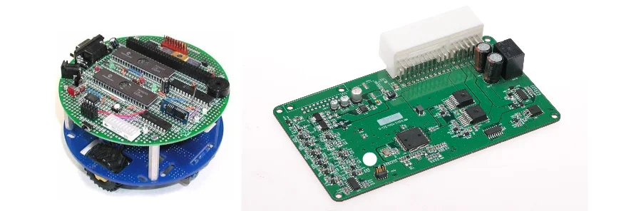
In the Industry 4.0 wave, industrial robots and automation systems have become the backbone of smart manufacturing. Their safe, stable, and efficient operation depends heavily on the performance of the control core—the PCB. Especially in human–robot collaboration and high-risk operations, dual-channel safety-control architectures have become an industry standard. To ensure robustness and reliability, a comprehensive Dual-channel safety control PCB checklist is indispensable. It is not only a design guide, but also a quality framework spanning concept design, physical implementation, and production validation—built to meet the harsh requirements of real-time industrial Ethernet such as EtherCAT and PROFINET.
As an industrial network engineer specialized in EtherCAT/PROFINET/CANopen, I know that the success or failure of a control system is often hidden in PCB-level details. From microsecond clock synchronization, to nanosecond-level jitter, to interference immunity in brutal EMC environments—each factor directly impacts robot responsiveness and safety redundancy. This article unpacks the core points of the Dual-channel safety control PCB checklist across real-time communication, PHY layout, EMC hardening, timing management, and test validation—helping you handle a complex design challenge. We also discuss how a deliberate Dual-channel safety control PCB stackup helps guarantee signal integrity, and how rigorous Dual-channel safety control PCB validation ensures compliance and reliability.
EtherCAT/PROFINET clock synchronization and jitter control: the foundation of real-time control
In industrial robotics control, real-time performance is the top priority. Multi-axis motion control and fast safety-stop response both require precise time coordination across nodes (drives, I/O, sensors). EtherCAT Distributed Clocks (DC) and PROFINET Isochronous Real-Time (IRT) both rely on IEEE 1588 PTP to control network jitter down to the nanosecond level.
The first job of the Dual-channel safety control PCB checklist is ensuring the PCB design can support this extreme time precision.
High-precision clock source and routing: the reference clock is usually provided by a high-stability crystal oscillator (TCXO/OCXO). In layout, keep it as close as possible to the main controller (FPGA or dedicated ASIC). Route its output as a critical differential pair with strict length/spacing matching. Ensure an unbroken reference ground plane underneath and avoid crossing any plane splits, so return paths remain clean and jitter does not increase.
PLL power decoupling: PLL blocks inside PHYs and controllers are extremely sensitive to power noise, which directly converts into clock jitter. Provide each PLL supply pin with a dedicated low-ESR, high-frequency decoupling network. Typically, multiple capacitor values (10nF, 100nF, 1uF) are used in parallel and connected with the shortest path to the pin and ground plane to form a low-impedance supply loop.
Distributed clock data-path integrity: in EtherCAT, timestamp information is embedded in Ethernet frames and captured precisely inside each slave’s ESC (EtherCAT Slave Controller). That means the PHY-to-ESC data path must have excellent SI. Distortion from impedance mismatch, crosstalk, or reflections can cause timestamp capture errors and break network synchronization. Therefore, simulation and analysis of these high-speed links is a required part of
Dual-channel safety control PCB validation.
PHY + magnetics layout: optimizing return paths and channel symmetry
The PHY is the bridge between the digital domain and physical cables, and its PCB layout directly determines communication quality and EMC performance. In dual-channel safety designs, two independent channels must be electrically isolated and performance-symmetric to make redundancy meaningful.
The golden-triangle placement: the relationship among PHY, magnetics, and the RJ45 connector is critical. Place them as close as possible in a compact “golden triangle.” Keep the path “PHY -> magnetics -> RJ45” direct, avoiding crossovers or detours. In particular, keep the differential pairs from PHY to magnetics (MDI/TD/RD) within 2 inches (~5cm) to reduce attenuation and noise pickup.
Differential symmetry and impedance control: Ethernet is differential, so symmetry requirements are strict. The P/N pair must be tightly length-matched, routed in parallel, and maintain constant spacing. Any mismatch in length or environment causes differential-to-common-mode conversion, turning energy into common-mode noise and an EMI source. Precise controlled impedance (typically 100Ω) is the baseline for signal quality, requiring a professional
Dual-channel safety control PCB stackupand impedance tools. With extensive High Speed PCB manufacturing experience, HILPCB can hold strict impedance tolerances.“Bob Smith” termination and grounding strategy: the center-tap grounding method of magnetics strongly affects EMC. A common approach is “Bob Smith” termination: connect through a series resistor (e.g., 75Ω) and a high-voltage capacitor (e.g., 1000pF/2kV) to chassis ground. This provides a discharge path for common-mode current while isolating DC and low-frequency noise. On the PCB, digital ground and chassis ground must be clearly separated and connected only at this single point to prevent ground-loop noise from coupling into sensitive digital circuitry.
🛡️ Dual-channel safety-control PCB: an end-to-end lifecycle flow from design to compliance
1. Protocol and SIL evaluation: define real-time and safety-level requirements, and select EtherCAT, CANopen, etc.
2. Anchor critical components: choose industrial-grade PHYs with hardware acceleration and high-isolation-voltage magnetics (e.g., 4kV).
3. Independent dual-path design: achieve full electrical isolation for power, clocks, and processors.
4. Stackup and impedance planning: run Dual-channel safety control PCB stackup simulations and use symmetric design to ensure transmission-line consistency across both differential-pair sets.
5. Route critical nets first: prioritize high-speed clocks and differential pairs; apply the 3W rule to reduce crosstalk.
6. Harden interface protection: enforce ESD, EFT, and surge protection arrays at external interfaces.
7. Precision process control: align with Dual-channel safety control PCB manufacturing and tightly control solder mask registration and lamination accuracy.
8. Closed-loop compliance testing: execute PCB validation and safety compliance tests, quantifying safety integrity.
ESD / surge / common-mode noise: a systematic approach to interface protection and EMI control
Industrial environments are full of EMI sources: EFT bursts from motor switching, surge events from lightning induction, and ESD. Without sufficient EMC design, PCBs can suffer data errors, communication dropouts, or even permanent damage. The Dual-channel safety control PCB checklist must include a systematic EMC protection strategy.
Cascaded protection at the interface: at the RJ45 entrance, deploy a complete multi-stage protection scheme:
- Stage 1: gas discharge tube (GDT) or high-power TVS diodes to shunt high-energy surge current.
- Stage 2: common-mode choke to filter common-mode noise on the differential pairs without affecting the differential signal.
- Stage 3: low-capacitance TVS diode arrays placed close to the PHY to clamp residual ESD/EFT energy and protect sensitive pins.
EMC layout considerations: placement matters as much as part selection. Protection devices must sit at the first line of defense—right next to the connector. The discharge path to ground must be short and wide for minimum impedance. In addition, a continuous guard ring along the PCB edge, tightly tied to chassis ground, helps block external EMI propagation along the board edge.
The importance of compliance testing: EMC cannot be guaranteed by theory alone—it must be verified by test. IEC 61000-4 series standards define detailed methods and severity levels. During development—especially for
Dual-channel safety control PCB low volumebuilds—pre-compliance testing is critical to expose issues early and avoid expensive delays at final certification. AchievingDual-channel safety control PCB complianceis a prerequisite for market entry.
Timing and real-time: co-designing buffers, interrupts, and hardware acceleration
Even with a perfect PHY, real-time performance can still suffer if higher-layer data processing becomes the bottleneck. This spans the full hardware–software pipeline: PHY reception, protocol-stack processing, and application response.
Leveraging hardware acceleration: modern industrial Ethernet controllers (e.g., EtherCAT ESC) integrate extensive hardware logic. Process Data Object (PDO) exchange is often mapped via hardware directly into dual-port RAM (DPRAM), so the CPU does not need to parse/forward every packet, drastically reducing latency. On the PCB, the controller-to-DPRAM data/address bus must have excellent SI, often requiring HDI PCB for high-density routing.
Controlling interrupt latency: when CPU involvement is needed (mailbox communication, state transitions), an interrupt is generated. The time from interrupt event to execution of the ISR is interrupt latency. Excessive latency breaks determinism. Plan interrupt priorities properly and route interrupt lines away from noise sources to prevent spurious interrupts.
Buffer/FIFO management: FIFOs are commonly used in the Tx/Rx path to smooth traffic and prevent packet loss during bursts. FIFO depth is a trade-off: too small risks overflow; too large increases inherent latency. This is a system-level decision, but it directly affects PCB routing density and power consumption.
Key reminder: core principles for dual-channel safety PCB design
- Physical isolation: power, ground, signals, and clocks must be physically separated between channels to avoid single points of failure.
- Performance symmetry: routing length, topology, and component placement should be as mirror-symmetric as possible so delay and response match.
- Independent clocks and cross monitoring: each channel should have its own clock source, with cross-monitoring circuitry so one channel can detect the other’s clock faults.
- Power redundancy and monitoring: provide independent power rails per channel with real-time voltage/current monitoring; anomalies must trigger a safe state.
- Strict DFM/DFA: consider Dual-channel safety control PCB manufacturing feasibility during design to ensure accurate and reliable build and assembly.
Conformance and interoperability: protocol-stack validation and test-jig design
After the first prototypes are built, validation becomes the most critical step. For industrial networking products, validation spans two layers: conformance and interoperability.
Conformance test: verifies strict compliance with protocol specifications (e.g., ETG.5001 for EtherCAT). Official organizations (ETG, PI) provide standardized tools such as the EtherCAT Conformance Test Tool (CTT). Tests cover PHY electrical characteristics, data-link state machines, and application-layer object dictionaries. Passing conformance is required for official certification and market access.
Interoperability test: conformance alone doesn’t guarantee perfect operation with devices from other vendors. Interoperability testing connects the DUT into complex networks with mixed masters/slaves across brands and runs long-duration, high-load tests to find compatibility issues—often in industry “Plugfests”.
Test jigs and automation: efficient testing requires dedicated test jigs that provide stable power, convenient interface access, measurement points, and support automation scripts. During
Dual-channel safety control PCB validation, test-jig design is as important as the PCB itself. HILPCB’s prototype assembly service can quickly build PCBA samples for validation and testing.
From design to manufacturing: low-volume production and compliance challenges
Turning a validated design into a reliable product is the final test, especially for high-reliability industrial control PCBs. Manufacturing details directly impact quality and lifetime.
Why DFM matters: incorporate manufacturing constraints early. Too-small pads or too-tight spacing can reduce yield. Early communication with the PCB manufacturer (e.g., HILPCB) to obtain process capability limits is the best way to prevent rework. This is particularly important for
Dual-channel safety control PCB low volumebuilds because tuning and optimization costs are higher per unit.Material selection and stackup control: industrial products typically require high-Tg FR-4 PCB to cover wider operating temperature ranges. In
Dual-channel safety control PCB manufacturing, lamination accuracy, dielectric stability, and copper-thickness uniformity are critical to achieving controlled impedance.Supply-chain and component management: key parts such as high-isolation magnetics, industrial connectors, and controller chips often have long lead times and limited sources. Before
Dual-channel safety control PCB low volumeor volume production, build a stable supply chain and buffer critical components. HILPCB’s turnkey PCBA service can help manage complex sourcing and inventory, simplifying production.
Frequently Asked Questions
Why is a dual-channel safety-control checklist so important in industrial robotics PCBs?
Because safety redundancy only works when both channels stay electrically isolated, time-deterministic, and performance-symmetric under EMC stress and manufacturing variation. Without a checklist, teams often miss hidden single-point failures in clocks, power, grounding, or interface protection.
Which PCB details most affect real-time Ethernet performance in dual-channel control?
The most sensitive details are clock-source stability, PLL decoupling, short PHY-to-magnetics paths, differential-pair symmetry, and clean return-path control. Small layout mistakes in those areas can increase jitter, disturb synchronization, and reduce channel consistency.
What validation work is needed before low-volume or volume production?
Teams should complete protocol conformance and interoperability tests, EMC pre-compliance, fixture-assisted functional validation, stackup and impedance checks, and a DFM review of creepage, isolation, and sourcing risk. That combination is what turns a working prototype into a deployable industrial product.
Conclusion
A high-performance, high-reliability industrial robot control system starts with a rigorous, comprehensive, end-to-end Dual-channel safety control PCB checklist. This checklist is more than a list of rules—it is systems engineering thinking: understand the nature of real-time communication, master every physical-layer detail, build EMC protection systematically, co-optimize hardware/software timing, and finally convert design intent into a rock-solid product through strict validation and precision manufacturing.
From precise Dual-channel safety control PCB stackup planning, to stringent Dual-channel safety control PCB compliance certification, to flexible and efficient Dual-channel safety control PCB low volume production, every step is challenging. By following the key points in this article and collaborating with an experienced PCB solution provider like HILPCB, you can better master these challenges and build a strong, reliable “heart” for industrial automation—successfully delivering on the Dual-channel safety control PCB checklist.