
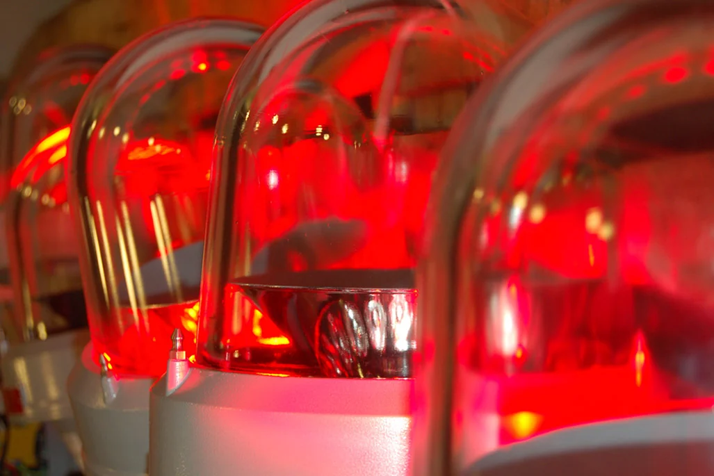
An explosion proof LED PCB is the board-level electronics platform used inside a certified hazardous-location luminaire to control ignition risk, thermal rise, insulation, corrosion, and long-term reliability. The PCB does not make a lamp "explosion proof" by itself; it supports the protection concept, testing evidence, and manufacturing consistency required for the final certified lighting assembly.
This guide is written for lighting OEMs, industrial fixture designers, and sourcing teams reviewing PCBs for oil and gas facilities, chemical plants, paint booths, grain or dust environments, mining support areas, and other hazardous locations.
Key takeaways
- A PCB is normally not certified as an explosion-proof product by itself. ATEX, IECEx, UL, CSA, or local hazardous-location approvals are usually evaluated at equipment, component, enclosure, or assembly level.
- The PCB must be designed around the equipment protection method: intrinsic safety, increased safety, encapsulation, flameproof enclosure support, non-sparking concepts, or a project-specific combination.
- Thermal design is a safety issue, not only an LED lifetime issue. The board must help keep component and enclosure surface temperatures below the required temperature-class limit under the rated ambient and fault assumptions.
- Metal core PCB, heavy copper, thermal vias, low-thermal-resistance dielectrics, and controlled LED placement can reduce hot spots, but the complete luminaire still needs thermal validation.
- RFQ data should include the hazardous-area zone/classification, gas or dust group, temperature class, enclosure concept, ambient range, LED power map, coating or encapsulation requirement, and test documentation needs.
In this guide
- What an explosion proof LED PCB is allowed to claim
- ATEX, IECEx, zones, and what they mean for PCB review
- Protection methods and PCB design impact
- Thermal design for T-class control
- Substrate selection: FR-4, metal core, copper core, and ceramic
- Creepage, clearance, insulation, coating, and encapsulation
- Smart, RGBWW, variable-white, and industrial control features
- Common failure modes in hazardous-lighting PCBs
- Manufacturing and test controls
- Cost drivers and RFQ checklist
- Why work with HILPCB
- Reference standards and frameworks
- FAQ
What an explosion proof LED PCB is allowed to claim
The most important design boundary is simple: the PCB supports explosion-protected equipment, but the final hazardous-location approval belongs to the complete product or certified subassembly. A bare LED board cannot prove enclosure flame paths, external surface temperature, impact resistance, ingress protection, cable-entry behavior, dust accumulation behavior, or installation conditions by itself.
That does not make the PCB a minor part. It is often where the highest heat density, insulation stress, current switching, LED binning, sensing, and control electronics meet the mechanical limits of a sealed industrial luminaire. If the PCB creates a hot spot, allows leakage across contamination, traps potting voids, or routes high-energy circuits too close to low-energy interfaces, the certification strategy can fail late in the project.
A strong explosion proof PCB review should answer four questions before layout is released:
| Review question | Board-level meaning | What should be documented |
|---|---|---|
| What protection concept is the luminaire using? | The PCB rules differ for intrinsic safety, increased safety, encapsulation, flameproof enclosure support, and non-sparking concepts | Ex concept, target market, certification route, enclosure assumptions |
| What hazardous atmosphere is expected? | Gas, vapor, mist, dust, or fiber hazards change temperature and ingress assumptions | Zone or class/division, gas/dust group, dust-layer assumptions if applicable |
| What is the thermal limit? | LED junction temperature is not enough; surface temperature and component temperatures matter | Target T-class or maximum surface temperature, rated ambient range, power dissipation map |
| What evidence does the certification body need? | PCB drawings alone are not enough | Stackup, material data, creepage/clearance report, coating/encapsulation process, thermal test plan, traceability requirements |
A useful wording pattern is therefore not "this PCB is ATEX certified." A safer and more accurate statement is: "This PCB is designed to support a hazardous-location LED luminaire certification package, with materials, spacing, thermal paths, and process controls reviewed against the selected equipment protection concept."
Project Boundary
HILPCB can support PCB fabrication, metal-core substrate selection, thermal-path review, DFM feedback, SMT assembly, coating or encapsulation coordination, and manufacturing documentation for hazardous-location lighting programs. Final ATEX, IECEx, UL, CSA, or other hazardous-location approval must be performed at the equipment or certified assembly level by the product owner and the selected certification body.
ATEX, IECEx, zones, and what they mean for PCB review
ATEX and IECEx are often mentioned together, but they are not the same object. ATEX is an EU regulatory framework for equipment and protective systems intended for potentially explosive atmospheres. IECEx is an international certification system based on standards for equipment used in explosive atmospheres. For a PCB project, both frameworks point to the same practical lesson: the board should be reviewed as part of an equipment safety case, not as a standalone marketing label.
Hazardous-area classification tells the PCB team how much conservatism to expect in energy limitation, insulation, thermal design, ingress protection, enclosure interface, and manufacturing documentation. The exact classification is normally determined by the site owner, system integrator, or safety engineer—not by the PCB supplier.
| Atmosphere type | Common zone terms | Meaning in plain language | PCB review impact |
|---|---|---|---|
| Gas, vapor, or mist | Zone 0 | Explosive atmosphere is present continuously, for long periods, or frequently | Board normally needs to support a very conservative system concept; high-power LED electronics are usually not placed directly in this zone without certified protection architecture |
| Gas, vapor, or mist | Zone 1 | Explosive atmosphere is likely to occur occasionally in normal operation | Spacing, temperature rise, enclosure interface, connection reliability, and fault assumptions become central review items |
| Gas, vapor, or mist | Zone 2 | Explosive atmosphere is not likely in normal operation, and if it occurs, it exists only briefly | The PCB still needs controlled spacing, component temperature review, and documentation matched to the selected protection method |
| Combustible dust | Zone 20 | Explosive dust cloud is present continuously, for long periods, or frequently | Dust ingress, surface temperature, dust-layer heating, creepage contamination, and cleaning assumptions become critical |
| Combustible dust | Zone 21 | Explosive dust cloud is likely occasionally in normal operation | Conformal coating, enclosure sealing, tracking resistance, and heat accumulation require early review |
| Combustible dust | Zone 22 | Explosive dust cloud is not likely in normal operation, and if present, only briefly | Manufacturing consistency and thermal margin still matter because dust can reduce cooling and increase surface temperature |
Temperature class is another critical input. For gases, T-class identifies the maximum surface temperature category of the equipment. The PCB team should treat T-class as a thermal design target for the complete product, not as a property of the bare board alone.
| Temperature class | Maximum surface temperature | PCB implication |
|---|---|---|
| T1 | 450°C | Rarely the limiting factor for LED PCB design, but component ratings still matter |
| T2 | 300°C | High-temperature material behavior, solder fatigue, and cable interfaces still need review |
| T3 | 200°C | Many polymer and coating systems begin to constrain design choices |
| T4 | 135°C | LED junction, driver IC temperature, and enclosure heat flow usually require careful validation |
| T5 | 100°C | Thermal margin becomes tight in sealed luminaires and high-ambient installations |
| T6 | 85°C | The strictest common gas T-class; PCB heat spreading, LED power density, and enclosure conduction must be reviewed very early |
For dust applications, the review should not simply copy the gas T-class table. Dust ignition risk depends on the dust type, cloud behavior, layer thickness, surface temperature, and cleaning conditions. If the fixture is intended for dust areas, the PCB package should include dust-specific assumptions from the certification plan.
Protection methods and PCB design impact
Different protection methods create different PCB priorities. A layout that makes sense inside a flameproof enclosure may be wrong for an intrinsically safe sensor circuit or an encapsulated driver module.
| Protection method | Core idea | PCB design focus | Common mistake |
|---|---|---|---|
| Intrinsic safety, Ex i | Limit electrical and thermal energy so a circuit cannot ignite the atmosphere under specified conditions | Low voltage/current, energy-limiting components, separation between intrinsically safe and non-IS circuits, controlled capacitance and inductance | Treating high-power LED strings as if they can be solved by spacing alone |
| Increased safety, Ex e | Prevent arcs, sparks, and excessive temperatures in normal service through enhanced construction | Secure connections, conservative spacing, high-integrity insulation, temperature-rated components, robust assembly | Using consumer LED spacing rules in a hazardous-location product |
| Encapsulation, Ex m | Encapsulate parts so ignition-capable circuits are isolated from the atmosphere | Component height control, potting flow, void prevention, thermal expansion, heat conduction through encapsulant | Assuming potting only adds protection and forgetting that it can trap heat |
| Flameproof enclosure support, Ex d | The enclosure contains an internal ignition and prevents flame transmission | PCB must manage internal heat, mechanical fit, connector locations, and serviceability inside the certified enclosure | Claiming the PCB is flameproof when the enclosure is the protection device |
| Non-sparking / restricted concepts | Reduce ignition-capable events under defined lower-risk conditions | Reliable contacts, controlled switching, low surface temperature, stable insulation | Using the term as a shortcut without matching the exact standard and zone/classification |
High-power LED lighting often combines several design disciplines. The LED load may be managed thermally through metal core PCB construction, the driver may need reinforced insulation and thermal derating, and a monitoring or communication circuit may require lower-energy routing. The protection method should be chosen first, then the PCB architecture should be built around it.
Thermal design for T-class control
Thermal management is the board-level issue most likely to become a certification bottleneck. In ordinary lighting, high temperature reduces luminous flux and shortens L70 lifetime. In hazardous-location lighting, high temperature can also reduce the safety margin against ignition and material degradation.
A sealed explosion-protected luminaire usually has limited convection inside the housing. The heat path is mostly conductive: LED junction → solder joint or thermal pad → copper land → dielectric layer → metal core or thermal plane → housing → ambient air. Every interface in that chain matters.
| Thermal design item | What to check | Why it matters |
|---|---|---|
| LED power map | Maximum wattage by LED channel, color, and dimming mode | RGBWW and variable-white fixtures can create worst-case heat in one channel, not only at full white output |
| Metal-core dielectric | Thermal conductivity, dielectric thickness, breakdown rating, and supplier data | The dielectric layer often dominates thermal resistance in MCPCB construction |
| Copper weight | 1 oz, 2 oz, 3 oz, or heavier copper depending on current and heat spreading | Higher copper can reduce localized hot spots, but it affects etching tolerance and cost |
| Thermal vias | Via pattern, fill type, annular ring, and wetting control | Vias can help spread heat in multilayer designs but may introduce assembly risks if not specified correctly |
| Driver placement | Distance between LED heat sources, driver ICs, sense resistors, and electrolytic capacitors | Driver components can create local hot zones even when LED pads look safe |
| Enclosure contact | Flatness, screw torque, thermal interface material, and contact pressure | A good PCB thermal design can fail if the housing interface is poor |
| Ambient rating | Rated ambient temperature and installation orientation | A fixture tested at one orientation or ambient may not represent the worst installation case |
The board should be reviewed using the temperature class and ambient range from the certification plan. A design intended for T6 at high ambient has a much narrower margin than a design intended for a less restrictive surface-temperature limit.
Practical review rule: do not approve the PCB stackup only from LED junction calculations. The review should include component case temperature, PCB hot-spot temperature, enclosure interface assumptions, and the maximum surface-temperature path required by the final equipment rating.
Substrate selection: FR-4, metal core, copper core, and ceramic
The substrate decision should be made from the heat path, insulation requirement, mechanical environment, and certification plan. Standard FR-4 can still appear in control, sensor, or low-power sections, but it is usually not the first choice for a high-power LED heat-spreading board in a sealed hazardous-location luminaire.
| Substrate route | Typical use in hazardous lighting | Strength | Main caution |
|---|---|---|---|
| Standard FR-4 | Low-power control boards, communication boards, sensor interfaces, auxiliary logic | Low cost, mature fabrication, easy multilayer routing | Poor thermal conductivity; not suitable as the primary LED heat path for high-power sealed luminaires |
| High-Tg FR-4 | Driver or control sections with elevated ambient temperature | Better thermal robustness than standard FR-4 | Still not a metal heat spreader; temperature rating does not equal heat dissipation |
| Aluminum MCPCB | Main LED engine boards for many industrial luminaires | Good cost-to-thermal balance, strong mechanical platform | Dielectric layer must balance thermal conductivity and insulation strength |
| Copper-core MCPCB | High power density LEDs, COB modules, compact industrial lights | Better heat spreading than aluminum routes in many demanding cases | Higher cost, heavier board, more process constraints |
| Heavy copper PCB | Driver boards, power distribution, high-current sections | Current capacity and lateral heat spreading | Etching tolerance, spacing, and soldering profiles must be controlled |
| Ceramic PCB | Specialized high-temperature, compact, or chemically demanding applications | High thermal stability and electrical insulation depending on ceramic family | Higher cost and different mechanical risk; not a universal replacement for MCPCB |
HILPCB can support substrate discussions across metal core PCB, high thermal PCB, heavy copper PCB, and ceramic routes when the project requires a more specialized thermal platform. The correct choice should come from the fixture architecture, not from a generic assumption that one material is always safest.
Creepage, clearance, insulation, coating, and encapsulation
Explosion-protected lighting is usually installed in places where moisture, dust, chemical vapor, vibration, and temperature cycling are normal. That means insulation reliability cannot be treated as a final DRC check. It must be part of the design concept.
Creepage and clearance values depend on working voltage, pollution degree, material group, protection concept, coating, encapsulation, and the exact standard being applied. The PCB supplier should not guess these values. The product owner or certification engineer should provide the required spacing rules, and the PCB drawing should make those rules inspectable.
| Insulation control | Board-level design action | Manufacturing control |
|---|---|---|
| Clearance | Maintain air distance between conductive features according to the approved design rule | AOI and design-rule review against released fabrication data |
| Creepage | Maintain surface path distance across laminate or coating surfaces | Clean surface finish, solder-mask registration control, contamination control |
| Slots and barriers | Add routed slots or physical separation where spacing cannot be achieved in plane | Dimensional inspection and burr control |
| Solder mask | Use as process protection, not as the only safety insulation unless accepted in the certification design | Mask thickness, registration, adhesion, and cure control |
| Conformal coating | Protect against humidity, condensation, corrosion, and dust contamination | Coating type, thickness range, coverage inspection, masking plan |
| Encapsulation | Physically isolate selected circuits and reduce exposure to atmosphere | Potting material, cure profile, void inspection, thermal expansion review |
Conformal coating and encapsulation should not be treated as interchangeable. A thin coating can help protect against moisture and contamination, but it is not automatically an Ex m encapsulation system. Encapsulation is a protection concept with material, thickness, void, and thermal requirements that must be reviewed as part of the certified equipment design.
For hazardous-location LED boards, coating selection is usually a tradeoff:
| Coating or encapsulant type | Typical advantage | Typical caution |
|---|---|---|
| Acrylic conformal coating | Easy processing and rework | Limited chemical and temperature resistance compared with stronger systems |
| Urethane coating | Better moisture and chemical resistance | Rework can be harder; cure control matters |
| Silicone coating | Good flexibility and temperature cycling behavior | Mechanical softness and contamination sensitivity must be reviewed |
| Epoxy encapsulation | Strong mechanical and chemical barrier | Can trap heat and stress components if thermal expansion is not managed |
| Silicone gel or rubber encapsulation | Flexible encapsulation and stress relief | Needs compatibility review with enclosure, outgassing, and temperature range |
Smart, RGBWW, variable-white, and industrial control features
Modern hazardous-location luminaires are no longer limited to fixed-output white light. OEMs may add DALI dimming, 0–10 V control, emergency lighting functions, status indication, condition monitoring, wireless service interfaces, RGBWW warning colors, or variable-white lighting for inspection areas.
These features add value, but they also add risk if they are inserted into an explosion-protected product without a board-level architecture review.
| Feature | PCB risk | Review action |
|---|---|---|
| RGBWW Light PCB | Multiple LED channels can create uneven heat distribution and unexpected worst-case color modes | Run thermal review for maximum channel stress, not only full-white operation |
| Variable White PCB | Warm and cool LED channels may age and heat differently | Review channel current, LED binning, thermal coupling, and CCT stability |
| Industrial Light PCB with dimming | Control input may connect to external field wiring | Review isolation, surge protection, creepage, and enclosure cable-entry assumptions |
| Wireless or sensor module | RF placement and digital noise can conflict with metal housings and LED drivers | Keep RF design separate from high-current switching loops and confirm enclosure effects |
| Emergency or battery-backed lighting | Charging circuits and cells add fault-energy and temperature concerns | Review battery certification, thermal spacing, protective circuitry, and serviceability |
| Facade Light PCB adaptation | Outdoor lighting priorities may not match hazardous-location safety priorities | Do not reuse decorative lighting layouts without rechecking spacing, thermal, and certification constraints |
| Strip Light PCB adaptation | Long flexible or linear boards may have voltage drop, hot-spot, and sealing issues | Validate each segment, connector, and installation condition; do not assume consumer strip rules apply |
A specialized lighting function should be added only after the protection method, thermal limit, and interface assumptions are clear. In hazardous-location design, "feature density" is not the same as product maturity.
Common failure modes in hazardous-lighting PCBs
The strongest way to review an explosion proof lighting PCB is to ask how it can fail. The table below is designed as a release checklist rather than a theoretical list.
| Failure mode | Typical board-level cause | Possible consequence | Prevention or review control |
|---|---|---|---|
| Local LED hot spot | Dense LED placement, weak dielectric, poor housing contact, uneven channel loading | T-class margin loss, accelerated LED aging, discoloration | Thermal simulation, power-map review, sample thermal measurement, enclosure contact validation |
| Driver IC overheating | Driver placed near LEDs or enclosed without heat spreading | Shutdown, flicker, premature failure, safety-margin reduction | Separate driver heat sources, add copper spreading, derate components |
| Creepage tracking | Contamination, moisture, dust, insufficient surface distance | Leakage current, carbonized path, insulation failure | Larger creepage, coating, cleaning, slots, contamination testing |
| Potting void | Poor encapsulant flow around tall components or connectors | Moisture pocket, partial discharge, reduced thermal transfer | Component keepout, potting vents, process validation, section inspection if needed |
| Solder joint fatigue | Vibration, thermal cycling, heavy components, poor support | Intermittent output or open circuit | Mechanical support, solder profile control, component staking where appropriate |
| LED color or brightness drift | High junction temperature, unequal channel aging, poor bin control | Unsafe visual indication or inconsistent lighting | Thermal balance, bin control, aging test, channel current review |
| Corrosion under coating | Flux residue, incomplete coating, chemical exposure | Leakage, open circuit, shorts | Cleaning validation, coating coverage inspection, material compatibility review |
| Connector or field-wiring fault | Inadequate strain relief, wrong terminal rating, poor separation | Arcing, heat, ingress path | Certified connector strategy, terminal torque review, spacing and enclosure interface check |
| ESD or surge damage | Long field wiring, insufficient protection, poor grounding | Latent failure or driver damage | Surge/ESD protection, grounding review, transient test plan |
| Documentation gap | Layout changed without certification file update | Approval delay or redesign | Revision control, material traceability, build records, change-notification discipline |
Manufacturing and test controls
A hazardous-location lighting board needs tighter process discipline than an ordinary LED board because the PCB may become part of the product's safety evidence. The required test plan depends on the equipment concept, but the following controls are commonly useful during board release.
| Control point | What it checks | Why it matters |
|---|---|---|
| Stackup and material verification | Laminate, metal core, dielectric thickness, copper weight, CTI or material group where specified | Confirms the build matches the spacing, thermal, and insulation assumptions |
| Impedance and high-current review | Control/signal integrity and current-carrying sections | Prevents overheating, noise coupling, and field failure |
| AOI and dimensional inspection | Trace integrity, solder-mask registration, slots, hole quality, component placement | Helps ensure creepage/clearance and assembly geometry match the release file |
| Electrical test | Opens, shorts, continuity, and isolation checks | Screens fabrication defects before assembly |
| Hi-pot or dielectric withstand testing | Insulation performance where specified by the product plan | Supports safety review for power and isolation circuits |
| Thermal sample measurement | Hot spots at rated input, worst-case LED mode, and rated ambient assumptions | Provides evidence for luminaire thermal validation |
| Coating inspection | Thickness, coverage, masking, bubbles, cracks, and cure | Prevents moisture and contamination paths |
| Potting process check | Fill, cure, voids, adhesion, and material compatibility | Ensures encapsulated circuits are not hiding thermal or insulation problems |
| Traceability | Material lots, process records, test data, revision history | Helps support certification files and failure analysis |
HILPCB can support PCB fabrication and SMT assembly workflows for LED lighting assemblies where the product owner defines the hazardous-location requirements. For higher-volume or build-to-print programs, turnkey assembly can include coordinated sourcing, assembly, inspection, and test steps according to the approved manufacturing package.
Cost drivers and RFQ checklist
Explosion proof lighting PCBs are often priced higher than ordinary LED boards because the project carries more process control, documentation, material selection, and test burden. The largest cost driver is not always the substrate itself; it is usually the combination of thermal margin, spacing, coating or encapsulation, traceability, and validation support.
| Cost driver | Why it changes price | How to control it |
|---|---|---|
| Metal-core or copper-core substrate | Specialized materials and processing | Provide realistic thermal targets instead of defaulting to the most expensive substrate |
| Heavy copper | More difficult etching, spacing, and soldering | Use heavy copper only where current or heat spreading requires it |
| High dielectric strength | Higher-performance MCPCB dielectric may cost more | Specify voltage, test requirement, and thermal conductivity together |
| Tight creepage/clearance | Larger board or slots may be required | Define the exact certification rule early |
| Coating or encapsulation | Adds material, masking, cure, inspection, and rework constraints | Provide coating type, keepouts, thickness, and inspection criteria in the RFQ |
| Thermal validation samples | Requires controlled builds and measurement setup | Define the exact power mode and ambient assumptions |
| Documentation and traceability | More process recording and lot control | State the certification and customer documentation requirements upfront |
| Mixed LED/control architecture | Multiple substrates or assembly processes may be needed | Split LED engine, driver, and control modules when it reduces risk |
RFQ data to provide
For a fast and useful quotation, send the following information with your Gerber or fabrication package.
Product and certification context
- Target market or certification route: ATEX, IECEx, UL, CSA, or local hazardous-location approval
- Hazardous area classification: zone or class/division
- Gas group, dust group, or known explosive material if available
- Required temperature class or maximum surface temperature
- Protection method under consideration: Ex i, Ex e, Ex m, Ex d enclosure support, non-sparking, or combined approach
- Rated ambient temperature range and installation orientation
PCB and thermal data
- Gerber, drill, IPC-356 netlist if available, stackup, and board outline
- LED power map by channel, including RGBWW or variable-white worst-case modes
- Driver topology, current levels, voltage rails, and switching frequency
- Required copper weight, metal-core type, dielectric target, or thermal conductivity target
- Enclosure contact area, screw locations, thermal interface material, and housing material if known
- Any thermal simulation or previous thermal test data
Manufacturing and protection requirements
- Solder mask color and reflectivity requirement for LED boards
- Coating or encapsulation material, thickness, keepout zones, and inspection needs
- Connector, cable, terminal, or field-wiring interface requirements
- Hi-pot, isolation, thermal, AOI, X-ray, coating, or custom functional test requirements
- Traceability, material certificate, and lot-control requirements
- Prototype quantity, pilot quantity, annual volume, and target lead time
Files for assembly
- BOM with manufacturer part numbers and alternates
- Pick-and-place file
- Assembly drawing
- Polarity and LED binning requirements
- Test procedure and acceptance limits
- Packaging and labeling requirements
Why work with HILPCB
Hazardous-location lighting projects usually fail late when the PCB package is treated like an ordinary LED engine. HILPCB helps reduce that risk by reviewing the board as a thermal, electrical, mechanical, and manufacturing package.
For explosion proof LED lighting programs, HILPCB can support:
- Metal core PCB and high-thermal LED substrate manufacturing for heat-spreading boards
- Heavy copper PCB for higher-current driver and power distribution sections
- DFM review for creepage, clearance, slots, solder-mask registration, mounting holes, and enclosure interfaces
- SMT assembly support for LED drivers, control circuits, sensors, connectors, and industrial lighting electronics
- Coating or encapsulation process coordination when the project file defines the material and inspection requirements
- Build documentation, revision control, and inspection data to support the customer's certification package
When the project is ready, send the hazardous-area requirements, stackup, LED power map, and assembly files through the Quote page. The best time to review the PCB is before the enclosure, driver, and LED channel layout have already been locked.
Reference standards and frameworks
The following standards and frameworks are useful references for hazardous-location lighting projects. The applicable list must be confirmed by the product owner, certification body, and target market.
- ATEX Directive 2014/34/EU — European Union
- IECEx Certified Equipment Scheme — IEC
- IEC 60079-0 — IEC
- IEC 60079-1 — IEC
- IEC 60079-7 — IEC
- IEC 60079-11 — IEC
- IEC 60079-18 — IEC
- IEC 60529 — IEC
- IEC 60598 — IEC
- IEC 61347 — IEC
- IEC 62384 — IEC
- IEC 62471 — IEC
- UL 844 — UL Standards & Engagement
- UL 8750 — UL Standards & Engagement
- NFPA 70 / NEC Articles 500, 505, and 506 — NFPA
FAQ
Can a PCB be ATEX or IECEx certified by itself?
Usually no. ATEX and IECEx certification normally applies to equipment, protective systems, components, or assemblies evaluated for use in explosive atmospheres. A PCB can support the certification file through controlled materials, spacing, thermal design, coating, encapsulation, testing, and traceability, but the final approval is normally for the complete luminaire or certified subassembly.
What is the biggest PCB design risk in explosion proof LED lighting?
Thermal margin is often the hardest risk to close. A sealed luminaire can trap heat, while LED boards, driver ICs, resistors, and power components all create local hot spots. The board must be reviewed against the required temperature class, rated ambient range, and enclosure heat path.
Is metal core PCB always required for explosion proof lighting?
Not always. Metal core PCB is common for high-power LED engines because it provides a strong heat path to the housing. However, low-power control boards, sensor boards, and communication boards may still use FR-4 or high-Tg FR-4 if the thermal and insulation requirements allow it. The substrate should be selected from the actual power map and certification concept.
Is conformal coating the same as encapsulation protection?
No. Conformal coating is a thin protective layer used for moisture, dust, corrosion, and insulation support. Encapsulation protection is a defined explosion-protection concept that uses an encapsulating compound to isolate circuits from the explosive atmosphere. The material, thickness, void control, thermal behavior, and process validation requirements are different.
Why do RGBWW and variable-white explosion proof lights need extra review?
Multi-channel LED boards can produce different worst-case thermal patterns depending on color mix and dimming mode. A design that is safe in full-white operation may still create a hot spot in a saturated color or inspection-lighting mode. Each channel should be reviewed for current, heat, optical function, and fault behavior.
What files should I send for an explosion proof LED PCB quotation?
Send Gerber files, drill data, stackup, BOM, pick-and-place file, assembly drawing, LED power map, hazardous-area classification, temperature class, rated ambient range, protection method, coating or encapsulation requirement, enclosure thermal-interface details, and any test or traceability requirements.
Can HILPCB guarantee that my finished luminaire will pass ATEX or IECEx?
No PCB supplier should guarantee final hazardous-location approval from the board alone. HILPCB can support PCB manufacturing, DFM review, thermal-path discussion, assembly, coating coordination, and documentation for the customer's certification package. The final approval must be completed through the product owner and the selected certification body.
Build the PCB package before certification becomes a redesign
Explosion proof LED lighting succeeds when safety, heat flow, insulation, enclosure design, and manufacturing evidence are planned together. The PCB should be reviewed before the product team freezes the LED layout, driver topology, coating plan, and housing interface.
Upload your files through the Quote page or send the hazardous-area requirements, Gerber package, BOM, LED power map, and assembly drawings to [email protected]. HILPCB can help review the board-level risks that usually become expensive when they are found after certification testing.