
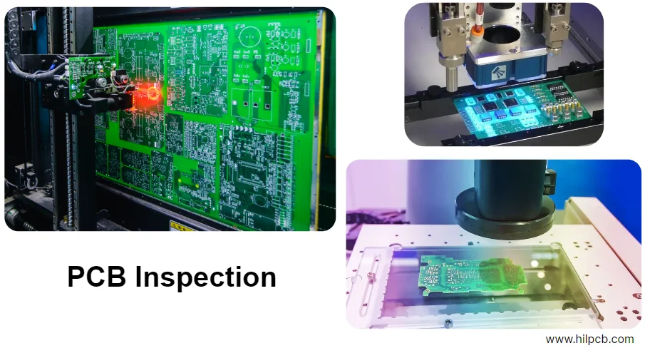
As 5G/6G communication technology accelerates, the mmWave band has become the key lever for higher network capacity and data rate. But that progress also brings unprecedented PCB design and fabrication challenges: loss, impedance control, material consistency, and complex interconnect structures. At these frequencies, tiny deviations at any step can cause a steep performance drop. In this demanding context, First Article Inspection (FAI) is no longer “just” dimensional and appearance checks—it evolves into a critical quality gate that proves mmWave circuit performance, interconnect reliability, and process stability. It is the bridge from design simulation to volume production, and the foundation for mastering high-frequency, low-loss communication PCBs.
From the perspective of a microwave measurement engineer, this article breaks down the FAI workflow for 5G/6G communication PCBs—focusing on de-embedding, probe-station and fixture calibration, S-parameter consistency validation, OTA testing, and failure analysis. We show how a systematic FAI approach ensures every high-frequency PCB meets the design targets precisely—supporting successful deployment of next-generation communication systems. This is both a technical guide and a practical mmWave antenna array PCB guide to help engineers and manufacturers win in the mmWave era.
The core of FAI: closing the loop from design validation to manufacturing consistency
Traditional FAI focuses on physical dimensions, hole location accuracy, and cosmetic defects. In mmWave applications, the scope expands dramatically. It becomes a comprehensive validation across electrical performance, material properties, and process stability—ensuring the first article fully meets design specifications and proving the manufacturing flow can repeatedly produce conforming boards.
For 5G/6G systems—especially antenna arrays and RF front-end modules—FAI matters because:
- A baseline for electrical verification: FAI validates key metrics via precise S-parameter measurement—characteristic impedance, insertion loss, return loss, etc. This is the first step in assessing SI requirements.
- Material-property consistency: mmWave circuits are extremely sensitive to dielectric constant (Dk) and dissipation factor (Df). By testing dedicated structures (e.g., resonators), FAI can back-calculate whether the real electromagnetic parameters match the datasheet or design input—critical when following a strict Rogers/PTFE hybrid stackup guide.
- Manufacturing stability assessment: Line-width control, lamination registration, and plating uniformity directly affect mmWave performance. FAI results reveal systematic process bias and provide data for process optimization.
- Quality assurance for low-volume builds: For RF front-end low noise PCB low volume projects, first-article success is decisive. A rigorous FAI process reduces risk in subsequent small-batch production and prevents large-scale scrap due to design or process gaps.
In short, modern communication-PCB FAI is a closed-loop system: it starts at design, uses precise measurement to validate the first article, feeds results back to manufacturing for correction, and ultimately ensures consistency and reliability in volume.
De-embedding: TRL/LRM/SOLT boundaries and error sources
In mmWave S-parameter measurement, we cannot probe the DUT port directly; fixtures, coax cables, and probes create transition structures. These transitions add their own loss, reflection, and delay, severely distorting results. De-embedding “strips” the test system’s influence via calibration to recover the DUT’s true network parameters. Selecting the right method is a prerequisite for FAI success—and a critical chapter in any mmWave antenna array PCB guide.
SOLT (Short-Open-Load-Thru): The classic calibration method uses known standards (short, open, 50Ω load, thru). It is common for coaxial measurements, but difficult for on-board planar mmWave testing because realizing ideal open/load standards on a PCB is extremely challenging. Parasitic C/L become non-negligible at high frequency, degrading calibration accuracy.
TRL (Thru-Reflect-Line): TRL and variants (TRM, LRM) are widely considered the “gold standard” for planar mmWave circuit testing. TRL does not rely on ideal loads/opens; it is based on transmission-line theory. It requires three standards on the PCB: a zero-length Thru, a high-reflection Reflect (often open or short), and a precisely known Line. By measuring these, the VNA can solve an error model and shift the reference plane to the DUT ports. TRL provides excellent accuracy, but its usable bandwidth is limited by the Line length—typically requiring a 20°–160° phase shift range.
LRM (Line-Reflect-Match): A TRL variant that uses a matched load (Match) in place of the Line, which can be easier when board space is constrained. However, accuracy depends strongly on the load’s matching quality and repeatability—still challenging for wideband applications.
In practice, TRL standards are often designed into dedicated test coupons to ensure measurement accuracy for critical high-speed channels. Understanding error sources—non-ideal SOLT standards, TRL line-length tolerance, probe-contact repeatability—is essential for reliable results.
De-embedding calibration method comparison
| Method | Core idea | Typical use | Main error sources |
|---|---|---|---|
| SOLT | Mathematically models the system using precisely known short/open/load/thru standards. | Coaxial connector systems; general testing at lower frequencies (< 40 GHz). | Non-ideal standards (especially open/load) at mmWave. |
| TRL | Defines reference planes via transmission-line theory by measuring Thru/Reflect/known Line. | Accurate de-embedding for planar lines (microstrip/CPW), especially wafer/PCB on-board probing. | Line-length accuracy; consistency of reflect standards (often open/short). |
| LRM | A TRL variant that replaces the Line with a matched load to simplify standards. | Space-limited cases where bandwidth is constrained. | Load matching accuracy and repeatability. |
Probe stations and fixtures: transition effects and repeatability control
The physical interface is the weak link of mmWave measurement—and one of the biggest contributors to test error. A stable, repeatable interface is essential to FAI because it directly determines how trustworthy your results are.
Probe station (Probe Station): For boards without connectors, on-board probing is the only option. A probe station provides micron-level positioning so high-frequency probes (typically GSG or GSSG) can land precisely on test pads. Probe selection, tip wear, contact pressure (over-travel), and alignment all significantly affect contact impedance and repeatability. During FAI, probe tips should be inspected regularly and repeatability tests should be performed to ensure the measurement system itself is stable.
Test fixture (Test Fixture): For boards with edge connectors (e.g., 2.92mm, 2.4mm), dedicated fixtures are required. Fixture design is a system task—mechanical tolerance, material choice, and EMC must be considered. The fixture body is typically metal for rigidity/shielding, while the PCB-contact region may use low-loss engineering plastics (e.g., PEEK) for precise alignment. The coax-to-microstrip transition is the core; any mismatch can create severe reflections. A fixture designed per mmWave antenna array PCB best practices should be optimized with 3D EM simulation to minimize transition effects.
Repeatability control (Repeatability Control): In FAI, repeatability can matter even more than absolute accuracy. You must ensure variation comes from the DUT, not the test setup. Key controls include:
- Torque wrench: Use a calibrated torque wrench on coax connectors to keep contact pressure consistent.
- Stable test environment: Keep cables fixed; avoid bending/movement that introduces phase shifts.
- Standard operating procedure: Define clear steps for DUT mounting, probe contact, and calibration verification to reduce operator error.
For mmWave antenna array PCB manufacturing, designing test-friendly interfaces and calibration structures is a prerequisite for smooth FAI execution and reliable data. For example, plan probe pad layout/size and reserve locating holes for fixtures during the design phase. Using high-performance materials such as Rogers PCB also supports high-repeatability measurements due to stable dielectric properties.
S-parameter consistency: bandwidth, bias, and temperature effects
S-parameters are the universal language of RF/microwave networks—and the core of FAI electrical verification. But a single S-parameter sweep is not enough; you must evaluate consistency and stability under defined boundary conditions.
Bandwidth and frequency resolution: 5G/6G signals occupy very wide bandwidth. FAI must cover the full operating band and harmonics. For example, a 28 GHz module may require a test range extending to 40 GHz or higher to check out-of-band resonances and parasitics. Adequate frequency resolution (sweep points) is essential to capture narrow resonances or steep filter edges.
Bias effects for active devices: Many RF front-end modules include active devices such as LNA, PA, or switches. Their S-parameters depend strongly on DC bias (voltage/current). During FAI, use a VNA with bias networks (Bias-Tee) and measure under rated operating bias. Monitor supply stability, since supply noise can modulate RF behavior and affect measurement. This is especially critical for RF front-end low noise PCB low volume validation, where performance is highly bias-sensitive.
Temperature drift and thermal management: mmWave devices—especially PA—dissipate significant power and heat up under operation. Semiconductor and dielectric properties change with temperature, shifting gain, phase, and matching. A rigorous FAI runs in a controlled temperature environment or uses a thermal chuck to actively control board temperature. If active control is not possible, measure after thermal stabilization and record ambient temperature in the report. Checking performance consistency across temperature is necessary for real-world reliability.
📊 S-Parameter KPI Monitoring Dashboard
mmWave OTA testing and anechoic-chamber validation
For PCBs that integrate antennas or antenna arrays, conducted tests alone are far from sufficient. Radiation performance—gain, pattern, beam direction—directly determines coverage and link quality. Therefore, over-the-air (OTA) testing is an indispensable part of FAI.
OTA tests are typically performed in an anechoic chamber to emulate a reflection-free free-space environment. The basic flow is:
- Test setup: Mount the DUT PCB on a low-reflection foam fixture and place it at the center of a high-precision turntable. The turntable rotates the DUT accurately in azimuth and elevation.
- Calibration: Replace the DUT with a known standard-gain antenna to measure path loss from the transmit antenna to the receiver as the reference baseline.
- Pattern measurement: The transmit antenna radiates a known CW signal toward the DUT. As the turntable rotates, a VNA or spectrum analyzer records received signal strength versus angle. Plotting these data yields the radiation pattern.
- Key parameter extraction: From the pattern, compute peak gain, 3 dB beamwidth, sidelobe level, and front-to-back ratio. For phased arrays, repeat across beam-steering states to verify scanning range and pointing accuracy.
OTA testing is the ultimate validation of mmWave antenna array PCB best practices. It evaluates not only the antenna elements, but also the combined performance of feed networks, phase shifters, and power dividers. For example, amplitude/phase mismatch across feed paths directly distorts the pattern and reduces gain. Following a precise Rogers/PTFE hybrid stackup guide is the basis for feed-network consistency, and complex arrays often require advanced fabrication such as HDI PCB to implement.
When consistency fails: localization and corrective actions
One of the most valuable roles of First Article Inspection (FAI) is catching and solving problems early. When results fall out of spec, fast and accurate root-cause identification is critical.
Root Cause Analysis (Root Cause Analysis): Failures typically originate from one of three areas—design, material, or manufacturing.
- Design issues: inaccurate simulation models, improper impedance-matching networks, insufficient EMC considerations, etc.
- Material issues: actual board Dk/Df deviates from design values; poor lot-to-lot consistency.
- Manufacturing issues: line/space out of tolerance, non-uniform resin flow during lamination, drill wander, poor plating, etc.
Failure localization techniques:
- Time-Domain Reflectometry (TDR): By launching a step edge and analyzing reflections, TDR converts frequency-domain S11 into a time-domain impedance profile. This lets engineers “see” impedance discontinuities along the path—connector transitions, vias, corners—so issues can be located quickly.
- Near-field scanning: Scanning above the PCB with small E-field/H-field probes visualizes EM field distribution, helping identify leakage, crosstalk paths, and EMI radiation sources.
- Physical Failure Analysis (PFA): If non-destructive methods cannot confirm the cause, destructive analysis may be required. X-Ray can check internal structures, and cross-sectioning under a microscope can reveal stackup registration, via geometry, copper thickness, and etch profiles—directly validating whether fabrication meets the design intent.
Corrective and Preventive Actions (CAPA): After pinpointing the issue, define and execute a corrective plan—layout updates, rule adjustments, process optimization with the PCB manufacturer for mmWave antenna array PCB manufacturing (e.g., etch compensation, lamination profile), or switching to more suitable substrates. After actions, rerun FAI to close the loop: “find → analyze → fix → verify”.
🔍 FAI failure diagnosis & failure analysis (FA) closed-loop flow
For SI deviations or process drift found in first-article inspection, execute systematic Root Cause Analysis (RCA) and corrective actions.
Verify VNA/TDR calibration status, fixture de-embedding validity, and test temperature/humidity to ensure data authenticity and repeatability.
Use 3D X-Ray to scan internal via anomalies; combine with TDR impedance profiles to locate reflection points; use SAM to check delamination risk.
Import measured S-parameters into ADS/HFSS and fit by tuning material Dk/Df and geometry to quantify the physical drivers of performance deviation.
Perform micro-sectioning and SEM on suspect areas to check lamination misregistration, hole-wall roughness, backdrill depth, and other fabrication details.
Define corrective actions: adjust impedance-line design, optimize etch compensation, or switch to higher-Tg materials. Update the control plan and rerun FAI for verification.
Data processing and reporting: from S-parameters to actionable insight
The final output of FAI is a detailed report. It is not only a pass/fail record, but also a key communication artifact connecting design, manufacturing, and test teams. A strong report turns complex measurement data into clear, actionable insight.
Data visualization: In addition to standard S-parameter plots (log magnitude, phase, group delay), the Smith chart is powerful for impedance-matching analysis. The S11 trajectory on the chart shows whether the network is capacitive or inductive and how far it is from ideal match.
Statistical Process Control (SPC): For RF front-end low noise PCB low volume FAI, multiple samples (e.g., 3–5 boards) are often tested. Statistical analysis of key metrics (e.g., S21 at specific frequencies) using mean and standard deviation gives an initial estimate of process capability (Cpk) and predicts volume consistency.
Comprehensive report contents: A complete FAI report should include:
- Test overview: DUT info, test date, test engineer, environmental conditions (temperature, humidity).
- Test setup: instrument models, cables, probes/fixtures, calibration method, calibration kit information.
- Results: clear plots of all S-parameters against specification limits; tabulated key-point values.
- Pass/Fail conclusion: explicit pass/fail for each test item.
- Analysis and recommendations: if failures occur, include preliminary FA and recommended corrective actions.
This report becomes part of the product development record and provides valuable historical data for future iterations and production quality control. For customers who need an end-to-end solution, Turnkey Assembly helps ensure smooth FAI execution and seamless data handoff across design, fabrication, and test.
Common Questions
Why is FAI for 5G/6G mmWave boards more than a dimensional inspection?
At mmWave frequencies, small shifts in materials, impedance, transition design, or process stability can change loss and matching enough to break system performance. FAI therefore has to confirm electrical behavior, material consistency, and manufacturing repeatability instead of only checking dimensions and appearance.
Why should de-embedding and calibration structures be planned early in the design?
The article shows that TRL, LRM, and related methods depend on well-defined coupons, reference planes, and test transitions. If those structures are not built into the PCB and fixture strategy early, later measurements cannot cleanly separate DUT behavior from probe, cable, or fixture error.
Why does probe and fixture repeatability matter so much in mmWave FAI?
When the test interface changes from one run to another, engineers cannot tell whether variation comes from the PCB or from the measurement setup. Stable probe contact, connector torque, fixture alignment, and environmental control are therefore part of the quality gate, not just test-lab housekeeping.
Why are OTA validation and failure-analysis loops both required before production ramp?
Conducted measurements alone do not prove that antenna arrays radiate with the expected gain, beam shape, and pointing accuracy. If results still miss target, FAI must also support root-cause analysis and corrective action so the team can fix the actual design, material, or manufacturing issue before volume builds.
Conclusion: FAI is the passport to success in the mmWave era
In summary, driven by 5G/6G communication, First Article Inspection (FAI) has evolved from a simple manufacturing-validation step into a complex systems engineering discipline spanning microwave measurement, material science, process control, and data analytics. It is not optional—it is the core safeguard for mmWave PCB performance, reliability, and manufacturability.
A successful FAI depends on deep understanding of de-embedding principles, strict control of test-interface repeatability, full awareness of environmental effects, and systematic diagnostic capability when issues arise. It is the solid bridge connecting mmWave antenna array PCB best practices design intent with high-quality mmWave antenna array PCB manufacturing reality.
At HILPCB, we understand how critical FAI is to project success. We not only provide advanced test equipment and experienced measurement engineers, but also embed FAI thinking into every step—from design review to final assembly. With one-stop services from prototype to Small Batch Assembly, we help customers navigate mmWave and low-loss interconnect challenges and bring innovations to market faster—reliably, and to the highest quality standard. On the road to future high-speed communications, rigorous First Article Inspection (FAI) is your most reliable passport.