
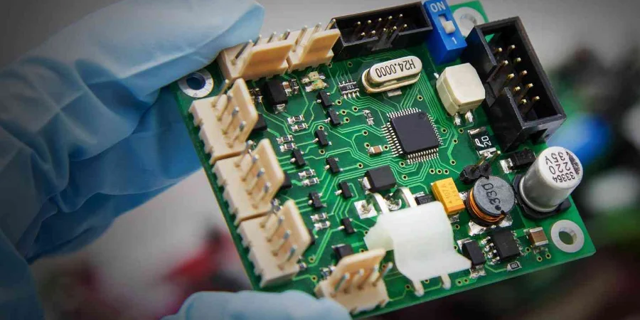
In 800G, 1.6T, and higher-speed data-center networks, optical modules often become the limiting factor for system performance and reliability. Inside a QSFP-DD or OSFP form factor, they integrate high-speed DSP, laser drivers, transimpedance amplifiers (TIA), lasers (EML/VCSEL), and complex micro-optics—all within an extremely compact volume. This level of integration and power density creates unprecedented PCB design and manufacturing challenges. In this context, First Article Inspection (FAI) is no longer just dimensional/BOM verification. It has evolved into a comprehensive system-level opto-electro-thermal validation gatekeeper that determines whether a product can move from prototype to scalable production.
From an opto-electro co-design engineer’s perspective, this article breaks down the FAI flow for data-center optical-module PCBs, focusing on the key challenges and verification strategies around high-speed SI, precision optical coupling, thermal management, and standards compliance. You’ll see how a successful FAI lays a solid foundation for QSFP-DD module PCB quality and ultimately protects data-center uptime.
The core of FAI: opto-electro co-validation beyond traditional PCB inspection
Traditional FAI emphasizes physical dimensions, stackup, hole accuracy, and BOM correctness. For optical modules, that is only the baseline. A modern First Article Inspection (FAI) must validate electrical, optical, thermal, and mechanical performance as one inseparable system.
That means FAI must verify:
- Electrical performance (SI/PI): Is the PAM4 eye open? Does channel insertion loss meet the budget? Is power noise within limits?
- Optical performance: Is laser-to-fiber coupling efficiency on target? Is optical output power stable?
- Thermal performance: Under full load, do key chips (DSP, drivers, TIA) stay below junction limits? Are thermal paths effective?
- Mechanical & standards compliance: Are assembly tolerances controlled across the PCB, cage, connectors, and heatsinks? Does the module fully meet QSFP-DD module PCB compliance, including CMIS management-interface functionality?
Only with this system-level scope can FAI expose deeper design/material/process issues early, preventing catastrophic failures in volume production.
Driver and TIA/LA: bandwidth, stability, and power isolation in the high-speed signal chain
An optical module’s signal chain starts at the Tx laser driver and ends at the Rx TIA/LA (transimpedance / limiting amplifier). This analog chain directly determines how well the module “sees” and “speaks.”
- Tx side: the driver converts PAM4 electrical signals from the DSP into modulation current for EML or VCSEL lasers. During FAI, use high-speed scopes/probes to measure eye quality directly at the driver output—eye height/width, linearity, and SNR. PCB impedance control, via design (e.g., Backdrill), and fan-out region layout near the driver all have decisive impact.
- Rx side: TIA converts photodiode current into voltage; LA amplifies and reshapes it. TIA is highly sensitive to power noise—small ripple can bury the signal. FAI must rigorously measure PDN impedance and noise spectrum on TIA supplies. This is especially important for TIA/LA receiver board quick turn programs where rapid iteration depends on quickly locating supply weak points.
- Power isolation: supplies between Tx and Rx, and between digital (DSP) and analog (Driver, TIA/LA) domains must be effectively isolated to prevent digital noise coupling. During FAI, use spectrum analysis to check noise crosstalk between rails and confirm that isolation bands, plane partitioning, and filtering work as intended.
FAI focus: validating the high-speed analog front end
- Eye validation: measure eye diagrams at the driver output and (if possible) at the TIA input to ensure sufficient PAM4 amplitude and timing margin.
- Power-noise analysis: use a high-bandwidth oscilloscope or spectrum analyzer to measure noise at Driver and TIA/LA power pins and confirm PDN performance against silicon requirements.
- Bandwidth and jitter testing: combine S-parameter measurement (VNA) with jitter decomposition to confirm end-to-end bandwidth and jitter budget compliance.
- Crosstalk evaluation: with adjacent channels active, evaluate inter-channel crosstalk and ensure it stays below the system tolerance threshold.
EML/VCSEL coupling: precision alignment and mechanical tolerance control in the optical path
Optical signal generation and transport depend on precise coupling between laser and fiber, often at micron or sub-micron scale. This places extreme demands on PCB dimensional stability and mechanical accuracy.
- OSA base and soldering: EML/VCSEL devices are typically packaged into an Optical Sub-Assembly (OSA) that solders to the main PCB via BGA or LGA. In FAI, use 3D X-Ray to check voiding, coplanarity, and alignment. Small tilt/shift can misalign the optical path and create large coupling loss.
- CTE matching: PCB CTE should match the OSA base material (often ceramic/metal) as closely as possible. Severe mismatch creates stress during temperature cycling, leading to solder fatigue or physical OSA movement. FAI uses thermal cycling to simulate long-term reliability and monitors optical power stability—critical for OSFP 800G transceiver board assembly reliability.
- Tolerance stack analysis: PCB flatness, OSA pad accuracy, and cage dimensions accumulate into final alignment of LC/MPO connectors to internal optics. FAI should use tools like CMM to measure key dimension chains across the full assembly and confirm they meet spec.
QSFP-DD/OSFP cage and thermal-design co-optimization
As module power climbs beyond 20 W, thermal management becomes a primary design constraint. The PCB is not only an interconnect carrier—it is a key part of the heat path.
- Thermal-path design: heat from DSP/Driver flows through Thermal Vias and copper planes into the module housing and out to the external heatsink. During FAI, test temperature distribution under full load using IR imaging and multi-point thermocouples to validate conduction paths and locate unexpected hotspots.
- Cage/heatsink interface: PCB thickness, outline, and local flatness determine contact quality with the cage and top heatsink. FAI must verify these interfaces so Thermal Pads/TIM are properly compressed for low thermal resistance. Strong QSFP-DD module PCB quality shows up here as tight mechanical tolerance and excellent flatness control.
- Airflow/environment emulation: wind-tunnel style thermal testing can emulate real switch/server airflow. By sweeping airflow and ambient temperature, FAI validates thermal headroom across boundary conditions.
HILPCB manufacturing capability: a solid foundation for optical modules
| Capability | Technical spec | Value for optical modules |
|---|---|---|
| Material selection | Full portfolio of Rogers, Megtron, Tachyon and other [High Speed PCB materials](/products/high-speed-pcb) | Enables low-loss PAM4 channels for 800G/1.6T data rates. |
| CTE control | Low-CTE materials and hybrid lamination options | Reduces stress mismatch with optical assemblies and improves long-term coupling reliability. |
| Tolerance control | Laser drilling, ±5% impedance control, strict thickness and flatness management | Protects high-speed differential performance and supports precision mechanical integration with cages/heatsinks. |
| Thermal-management solutions | Via copper fill, embedded copper blocks, heavy copper | Builds efficient vertical heat paths and lowers key-chip operating temperature. |
PAM4 channels: combined constraints and validation across SI/PI/EMI
PAM4 doubles the bit rate compared to NRZ, but it significantly reduces tolerance to noise and channel impairment. PAM4 FAI must therefore be comprehensive.
- Signal Integrity (SI): the core FAI task is using a VNA to measure channel S-parameters from the connector to package pads—especially insertion loss (IL) and return loss (RL). Results must match simulation models closely to confirm manufacturing meets design intent. Unexpected loss can fully close the eye.
- Power Integrity (PI): PAM4 levels demand a stable voltage reference. Under worst-case patterns (e.g., all lanes switching 00→11 simultaneously), FAI verifies that Voltage Droop stays within limits. This also depends on precision SMT Assembly so decoupling capacitors perform as intended.
- EMI: high-speed radiation is a major EMI source. During FAI, scan the module in an anechoic chamber to ensure compliance with FCC/CE requirements—essential for QSFP-DD module PCB compliance. Plane integrity, shielding design, and connector grounding are key controls.
CPO evolution: new FAI challenges for low-loss Co-packaged optics baseboard
As data rates move to 3.2T/s and beyond, the limits of pluggable modules become more apparent. Co-packaged Optics (CPO) places optical engines around the switch ASIC, shortening electrical interconnect length to reduce power and latency.
This architectural shift creates the need for a low-loss Co-packaged optics baseboard: large form factor, high layer count, and simultaneous support for ultra-high-speed electrical links and precision optical interconnect (e.g., waveguides).
FAI for CPO baseboards faces new challenges:
- Opto-electrical integration validation: FAI must measure both electrical and optical performance—waveguide loss, grating-coupler efficiency, and interconnect quality between optics engines and ASIC (e.g., HBI).
- Large-scale PDN: powering hundreds of ASIC cores and dozens of optical engines makes PDN extremely complex. FAI must validate supply stability and thermal distribution under kilo-amp-level currents.
- Material and process limits: low-loss Co-packaged optics baseboard requires top-tier ultra-low-loss materials plus ultra-precision manufacturing. FAI becomes the final verdict on whether these materials/processes perform stably in real hardware. HILPCB has deep experience with premium materials such as Rogers PCB and can support CPO development effectively.
HILPCB assembly advantages: accelerating your optical-module innovation
- One-stop service: from PCB fabrication to [Prototype Assembly](/products/small-batch-assembly), enabling a seamless flow and shortening R&D cycles for programs like TIA/LA receiver board quick turn.
- Precision placement capability: advanced equipment and experience for 01005 parts, high-density BGA, and optical components—key for successful OSFP 800G transceiver board assembly.
- Professional engineering support: our engineers understand opto-electro co-design challenges and provide practical guidance in DFM/DFA to improve yield at the source.
- Flexible volume support: from a few FAI prototypes to small pilot runs, we provide flexible and efficient production support.
Conclusion: FAI is the required path to high-performance optical modules
For modern data-center optical modules, First Article Inspection (FAI) extends far beyond traditional PCB inspection. It is a complex, cross-disciplinary system engineering activity—the critical bridge between simulation/design intent and scalable production. A successful FAI validates not only PCB build quality, but the performance and reliability of the entire opto-electro-thermal system.
Whether you are ensuring today’s QSFP-DD module PCB quality or exploring next-generation low-loss Co-packaged optics baseboard, a strict and comprehensive FAI process is indispensable. It exposes design defects, material issues, and process drift early—saving precious R&D time and major rework cost. Choosing a partner like HILPCB—one that understands opto-electro co-design and can deliver one-stop PCB + precision assembly—can be the key to success in high-speed optical interconnect.
Common Questions
Why is FAI so important for data-center optical modules and CPO hardware?
Because these products combine extremely fast electrical channels, sensitive optical paths, tight thermal limits, and very small process tolerances. FAI is the first point where all of those design assumptions are checked on real hardware instead of only in simulation.
Why must FAI validate optical alignment and electrical performance together?
High-speed optical modules only work well when optical coupling, signal integrity, power delivery, and assembly accuracy all support each other. Looking at only one side can hide system-level issues that later reduce bandwidth, margin, or yield.
Why do cage, connector, and thermal tolerances matter during FAI?
Mechanical fit and thermal behavior directly affect insertion loss, mating reliability, cooling efficiency, and long-term stability. FAI helps confirm that the assembled module still meets targets once real connectors, cages, heat sinks, and production tolerances are involved.
How does early FAI reduce risk for high-speed interconnect products?
It exposes layout errors, material variation, assembly drift, and interface problems before the design reaches pilot or volume manufacturing. That shortens debug cycles and prevents expensive rework on advanced optical-module programs.