
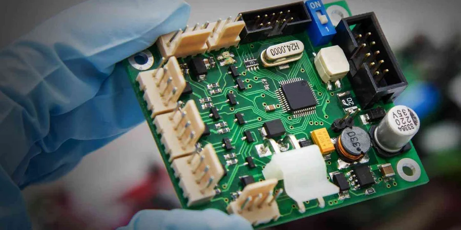
In today’s data-driven world—from data centers to AI accelerators—112G/224G SerDes PAM4 links are becoming the norm. For high-speed signal integrity (SI) engineers, that means margins are compressed to the extreme: tiny manufacturing deviations can break the entire channel. Between design intent and mass production stands a critical quality gate—First Article Inspection (FAI). For high-speed PCB, FAI is no longer “dimensional inspection”; it is the core validation step that proves design intent has been translated into physical reality. A strong FAI process is the foundation for surviving ultra-high-speed and low-loss challenges—and for turning a design into commercial success.
For complex High-Speed PCB, FAI must be tightly coupled to early DFM/DFT/DFA review, validating every step from material selection and stackup build to precision assembly. This is not only verification—it is a full capability audit of the manufacturing and assembly chain. In a one-stop Turnkey PCBA model, the depth and rigor of FAI directly determine final performance and reliability.
What is First Article Inspection (FAI) and why is it special for high-speed PCB?
First Article Inspection (FAI) is a formal, systematic verification process to confirm that production flow, tooling, and documentation can consistently build products that meet all engineering requirements (drawings, BOM, specifications, etc.). Before volume production, FAI typically inspects the first 1–5 units to capture manufacturing deviations and process defects early.
But when the target is a PCB carrying 112G PAM4, FAI changes qualitatively. It’s no longer just “are hole sizes and board thickness within tolerance?” For high-speed PCB, FAI must answer a deeper question: “Can this board reliably transmit signals at the target data rate?”
That unique meaning shows up in four dimensions:
- Performance-driven verification: traditional FAI focuses on geometry; high-speed FAI must validate electrical performance—TDR impedance, material Dk/Df, and critical via cross-sections.
- End-to-end process chain audit: high-speed performance is the result of design + materials + fabrication + assembly. FAI must review lamination and impedance control for the bare board and also reflow profiles and BGA quality for PCBA.
- A front-loaded firewall: in high-speed programs, a failed spin can cost millions and months. FAI prevents issues from scaling into volume and maximizes business-risk avoidance.
- A bridge between design and manufacturing: FAI reports provide the most objective language between designers and manufacturers—data and images that show whether design intent is realized and where to optimize.
For professional manufacturers like Highleap PCB Factory (HILPCB) offering Turnkey PCBA, FAI is the point where performance commitments become measurable, ensuring every delivered board can meet SI requirements.
How FAI validates the core elements of high-speed SI
An SI-aware FAI must go deep into the physical layer and quantify the drivers of signal quality with precision measurement and analysis—so results match simulation models and design specs.
1. Impedance control and TDR
Impedance discontinuities create reflections and shrink eye openings. TDR is non-negotiable in high-speed FAI.
- What to verify: measure single-ended and differential impedance on coupons.
- Acceptance: within design tolerance (often ±7% or tighter ±5%).
- Deep analysis: don’t stop at the final impedance number—inspect TDR waveforms. Small ripples can indicate etch non-uniformity or dielectric thickness drift.
2. Stackup and material verification
Material Dk/Df determine propagation speed and loss. For 56G/112G+, ultra-low-loss materials like Megtron 6 and Tachyon 100G matter.
- What to verify: cross-section to measure dielectric thicknesses against the stackup drawing; verify material model vs PO and supplier certificates.
- Acceptance: layer thickness tolerances meet spec; material models match exactly.
- Key challenge: Fiber Weave Effect causes local Dk variation. Advanced FAI evaluates spread glass behavior to protect impedance and delay consistency.
3. Via and transition structure analysis
In multilayer HDI PCB, vias are major discontinuities. Physical via validation is a core FAI task.
- What to verify: microsection inspection of drill quality, copper plating thickness/uniformity, and Back-drilling stub length.
- Acceptance: plating meets IPC (often >20 μm); backdrill stubs are tightly controlled (e.g., <10 mil) to reduce HF resonance.
- HILPCB practice: beyond stub length, we check barrel smoothness and plating adhesion—critical for long-term reliability.
By validating these SI fundamentals, FAI connects simulation assumptions to physical reality—ensuring the high-speed channel has a solid performance foundation.
Standard FAI vs. SI-aware high-speed FAI
| Item | Standard FAI focus | SI-aware high-speed FAI focus |
|---|---|---|
| Impedance control | Report provided (yes/no) | TDR waveform analysis, tolerance compliance (±5%), intra-/inter-layer consistency |
| Stackup/material | Overall thickness, material model check | Measured dielectric thickness per layer, Dk/Df verification, glass style, resin content |
| Via structure | Hole size, positional accuracy | Microsection, backdrill stub length, copper thickness/uniformity, aspect ratio |
| Surface finish | Type compliance (e.g., ENIG) | Ni/Au thickness uniformity, HF loss impact assessment (e.g., consider ENEPIG) |
| Trace geometry | Line width/spacing compliance | Diff-pair intra/inter spacing consistency, etch factor control, trapezoid-effect analysis |
Seamless link: from DFM/DFT/DFA review to FAI
An effective FAI is not isolated. It starts with early design involvement. A thorough DFM/DFT/DFA review is the foundation: it reviews Gerber and BOM from the fabrication/assembly perspective and fixes process traps before they become expensive failures.
DFM/DFT/DFA review and FAI form a “predict and verify” closed loop:
- Predict (DFM/DFT/DFA): during design, HILPCB engineers use CAM tools and manufacturing experience to analyze Gerber/BOM. Examples: check BGA pad designs vs IPC to avoid bridging/opens; evaluate whether diff-pair routing can meet tight etch tolerance for impedance stability; verify test point accessibility and prepare for Boundary-Scan/JTAG.
- Verify (FAI): FAI confirms those changes in the physical domain. If DFM recommends solder mask opening changes for BGA yield, FAI uses X-Ray images and data to confirm voiding/shape improvements. If DFM optimizes stackup for impedance, TDR results become the final verdict.
The value is shifting from “after-the-fact fixes” to “prevention up front”—reducing major issues found during FAI, shortening development cycles, and lowering total cost. It reflects the evolution of a mature PCB manufacturer from passive builder to proactive problem-solving partner.
FAI’s role inside a Turnkey PCBA workflow
In Turnkey PCBA, the customer assigns PCB fabrication, component sourcing, and SMT assembly to one supplier. This simplifies supply-chain management while raising the bar on the supplier’s quality control. In this context, FAI is the central “handoff hub” between stages.
FAI in Turnkey PCBA works across multiple layers:
- Fab FAI (bare-board): before assembly, validate stackup, impedance, materials, and other SI-relevant physical characteristics.
- IQC FAI (components): in Turnkey, first-lot inspection of critical components (high-speed connectors, FPGA, SerDes) is essential—model/lot/packaging verification and spot functional checks to prevent board-level failures.
- Assembly FAI: the core step after first build:
- Placement & orientation: AOI + manual checks to confirm part model, position, and orientation match BOM and drawings.
- Solder quality: X-Ray for BGA/QFN to assess shorts, opens, voiding, etc.
- Process parameter locking: record and verify paste print thickness and reflow profiles for stability and repeatability.
With a staged, full-coverage FAI flow, a Turnkey PCBA supplier keeps each transformation from bare board to assembled board under control—setting the baseline for stable volume production.
🛡️ HILPCB premium one-stop QA closed-loop
From design-risk identification to real-time SPC in volume production, build a fully traceable zero-defect quality system.
Identify DFM/DFT risks in NPI and optimize mask openings and probe layouts to ensure manufacturability from the start.
First-panel impedance tests, stackup microsections, and Tg verification to ensure baseboard physical properties match design standards.
Verify BOM with first-article inspection tools, and use X-Ray to validate BGA solder quality—locking the mass-production baseline.
Integrate ICT, FCT, and Boundary-Scan chain tests, plus 3D AOI, to achieve 100% electrical and visual coverage.
Use Cp/Cpk control to dynamically tune soldering and placement parameters and ensure long-term consistency in volume production.
Using Boundary-Scan/JTAG to increase FAI coverage
As pin pitch shrinks and packages get more complex (BGA, LGA), visual inspection, AOI, and even flying probe cannot fully cover all joints—especially hidden bottom-side joints. Boundary-Scan/JTAG (IEEE 1149.1) becomes a key tool to raise FAI coverage.
Boundary-Scan integrates test cells at device pins and chains I/Os. Through TAP, you can control and observe pin states. In FAI it delivers:
- Interconnect test: detects opens (cold solder, Head-in-Pillow) and shorts (solder ball bridging) between BGA pins. Running JTAG interconnect tests on the first build can confirm electrical connectivity for all testable nets—something X-Ray cannot do (X-Ray sees geometry; JTAG verifies continuity).
- Covering X-Ray blind spots: X-Ray finds bridging and size variation well, but for defects like Head-in-Pillow where a ball appears to contact but fails metallurgical bonding, X-Ray can miss it. JTAG identifies it as an open.
- In-system programming and validation: for FPGA/CPLD, JTAG supports in-system programming during FAI and immediate verification—combining hardware and firmware validation steps.
Making Boundary-Scan/JTAG a standard step in Assembly FAI greatly improves depth and reliability. It complements AOI and X-Ray: AOI checks visible placement, X-Ray inspects hidden joint morphology, and JTAG validates electrical connectivity.
How FAI ensures reliability of special processes
Modern high-speed PCB often require mixed processes. FAI must be flexible and professional enough to validate these special processes are executed correctly.
1. Selective wave soldering
When a dense SMT board includes a few high-power through-hole connectors or parts, Selective wave soldering is ideal.
- FAI validation focus:
- Thermal shielding effect: ensure nearby SMT parts (especially BGA and small passives) are not damaged or shifted by thermal shock.
- Through-hole fill: microsection to confirm adequate solder fill to IPC-A-610 Class 2 or Class 3.
- Flux residues: verify cleanliness around the soldered area to avoid corrosive residue.
2. Conformal coating
For products in harsh environments (moisture, salt fog, vibration), Conformal coating is essential.
- FAI validation focus:
- Thickness & uniformity: measure coating thickness at multiple regions to confirm spec and distribution.
- Coverage integrity: UV inspection to confirm protected areas are fully covered while connectors/test points are properly masked.
- Adhesion test: cross-hatch adhesion test to validate bonding strength.
For special processes, FAI is not a binary check—it is quantitative evaluation of parameters and execution quality. FAI reports should record key process parameters (nozzle type, solder temperature, conveyer speed; coating type and cure method/time). These become the product’s “process DNA” and a traceable baseline for stable production.
High-speed PCB FAI checklist (key points)
- Request and review TDR reports: focus on impedance values, tolerance, and waveform smoothness.
- Require microsection analysis for critical vias: check backdrill stubs, plating quality, and dielectric thickness.
- Verify material certificates: confirm the specified low-loss laminate model, vendor, and lot.
- Review X-Ray reports: focus on BGA voiding %, coplanarity, and alignment.
- Confirm JTAG test results: ensure 100% pass connectivity for critical nets (DDR, PCIe).
- Validate special process parameters: reflow profiles, coating thickness, etc.—recorded and within spec.
Reading the FAI report: what high-speed designers must focus on
A detailed FAI report may include dozens of pages of data, charts, and photos. High-speed designers should focus on the signals that predict SI success.
Dimensional report: beyond outline and thickness, focus on SI-critical geometry:
- Critical trace width/spacing: especially differential pair W/S—directly impacts impedance.
- Backdrill stub length: a key HF parameter that must stay within spec.
- BGA pads and solder-mask openings: affects solder reliability and consistency.
Material & stack-up report:
- Certificate of Conformance: include original laminate supplier documentation.
- Microsection data: compare measured dielectric/copper thicknesses layer-by-layer against stackup. Any out-of-tolerance drift can shift impedance.
Electrical test report:
- TDR/VNA plots: don’t only read pass/fail. Spikes/dips on impedance curves indicate physical defects even when averages remain within tolerance.
- VNA data: for 28G+ designs, require S-parameter reports (insertion loss, return loss). Compare measured channel loss to simulation budgets.
Assembly quality report:
- X-Ray images: inspect BGA ball roundness, size consistency, voiding and %, etc.
- AOI defect list: confirm misplacement, tombstoning, wrong parts, etc., are corrected on first builds.
A great FAI report is not just data—it is transparency of process capability. Customers can demand clear, complete, traceable reporting. Partners like HILPCB proactively provide detailed reports and engineering interpretation to ensure design intent is realized.
Beyond FAI: building continuous production quality control
First Article Inspection (FAI) validates “the first time,” but how do you ensure the 10,000th unit matches the first? You need a continuous Quality Assurance (QA) system. FAI is the starting baseline.
- Process locking: after FAI, lock all key parameters—lamination temperature/pressure, SMT placement speed, reflow profiles—and enforce them in volume.
- SPC: continuously monitor key parameters (impedance, etch width, copper plating thickness). Control charts detect drift early so issues are corrected before escalation.
- Scaled automated inspection: in volume, AOI and AXI move from sample tools to inline guardians for every board—ensuring assembly consistency.
- Periodic ORT: pull samples for tougher reliability tests (thermal cycling, vibration, burn-in) to confirm lifecycle stability.
A responsible manufacturer treats FAI success as the beginning of a long-term quality commitment. Using the FAI baseline plus SPC, automated inspection, and ongoing reliability validation, you can maintain a comprehensive QA system and ship products with confidence.
Common Questions
Why is FAI such a critical gate for 112G and 224G high-speed PCB programs?
At these data rates, small deviations in impedance, stackup thickness, via quality, or assembly execution can collapse channel margin quickly. FAI is the first point where the team confirms that the physical build still matches the assumptions behind SI simulation and loss budgeting.
Why must DFM/DFT/DFA review and FAI be treated as one closed loop?
The article frames DFM/DFT/DFA as the prediction stage and FAI as the verification stage. Reviewing manufacturability, testability, and assembly risk early only creates value if the first build is then measured against those decisions and used to confirm whether the intended corrections actually worked.
How does Boundary-Scan/JTAG improve first-article coverage on high-speed assemblies?
JTAG checks hidden interconnect integrity that visual inspection, AOI, or even X-ray cannot fully prove, especially under large BGA and LGA packages. That makes it a practical way to detect opens, shorts, and weak electrical connections on critical nets before the program moves into broader production.
What should engineers focus on after the first FAI report passes?
Passing the first report is only the baseline. Teams still need to lock process parameters, monitor drift with SPC and inline inspection, and keep reliability checks active so the same electrical and assembly quality can be held from pilot builds into volume production.
Conclusion: FAI is the key quality gate for high-speed PCB success
In high-speed SI PCB development and manufacturing, First Article Inspection (FAI) plays the role of an essential “quality gatekeeper.” It has evolved beyond dimensional checks into a comprehensive engineering validation activity combining electrical performance verification, materials analysis, precision process control, and advanced test techniques.
From rigorous DFM/DFT/DFA review to detailed inspection across the full Turnkey PCBA flow—and by using advanced methods like Boundary-Scan/JTAG to improve test coverage—a successful FAI process systematically lowers risk, protects performance, and lays a solid foundation for volume production. Whether validating Selective wave soldering reliability or ensuring Conformal coating uniformity, FAI is the bridge between design blueprints and real-world excellence.
Choosing a service provider like Highleap PCB Factory (HILPCB) that understands high-speed SI and has strong integrated manufacturing capability means you get more than an FAI report—you get an end-to-end quality commitment. Work with our expert team to build a robust QA plan for your next high-speed project and win in a competitive market.