
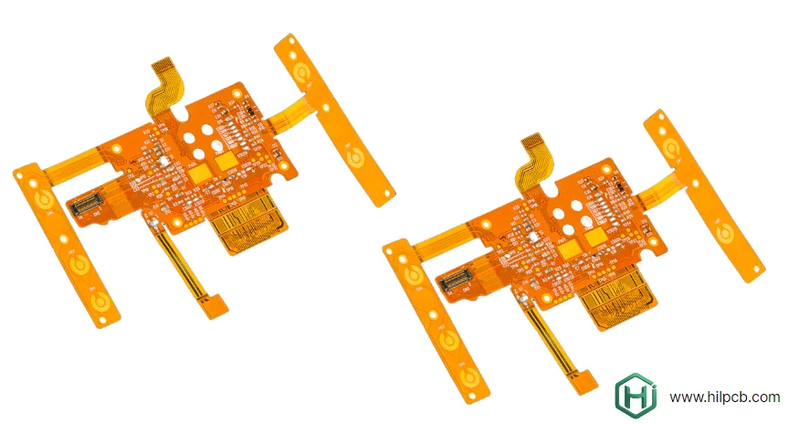
A flexible PCB, or FPC, is a printed circuit built on a bendable dielectric film so it can route signals and power through thin, lightweight, three-dimensional spaces. Reliable flexible PCB solutions begin by defining whether the circuit bends only during installation or repeatedly during operation, because those use cases require different copper, stack-ups, routing, and validation.
Key Takeaways
- “Flexible” does not automatically mean “dynamic.” A bend-to-install circuit and a continuously moving flex cable should not share the same design rules or qualification plan.
- Repeated-flex zones generally favor thin constructions, rolled-annealed copper, smooth conductors perpendicular to the bend axis, and no pads, vias, components, stiffener edges, or abrupt width changes in the active bend.
- Bend radius is a product-specific output, not a universal multiple of board thickness. Layer count, copper type and thickness, dielectric, adhesive, coverlay, bend direction, cycle count, temperature, and motion profile all matter.
- Solid copper planes improve shielding and return continuity but increase bending stiffness and strain. Cross-hatched planes may improve flexibility, while changing impedance, shielding, and current capacity.
- Stiffeners support connectors and components; they do not make a bend area stronger. A poorly placed stiffener edge creates a stress concentration and can shorten flex life.
- Production testing must be tied to expected failures. Electrical test finds opens and shorts, but only a representative bend test can validate the specified motion, radius, speed, and cycle life.
On this page
- What is a flexible PCB used for?
- Is the application static, service-flex, or dynamic?
- Which flexible PCB stack-up should you choose?
- How should a dynamic bend area be routed?
- How are stiffeners, coverlay, and connectors designed?
- Can flexible PCBs carry high-speed signals?
- How is heat managed on a flex PCB?
- How are flexible PCBs manufactured and assembled?
- What flex PCB failures should testing prevent?
- How should medical and automotive flex circuits be specified?
- What drives flexible PCB cost and lead time?
- What belongs in a flexible PCB RFQ?
- Reference standards and scope
- Why manufacture flexible PCBs with HILPCB?
- FAQ
What is a flexible PCB used for?
A flexible circuit replaces part of a wire harness, ribbon cable, connector chain, or rigid-board interconnect with a repeatable etched conductor pattern. It can reduce mass and assembly steps, control routing, fit around mechanical features, and connect rigid electronics across hinges or moving mechanisms.
Common applications include camera modules, displays, wearables, sensors, printers, robotics, battery packs, medical instruments, automotive interiors, aerospace electronics, and compact consumer products. The application name alone does not establish reliability: a wearable sensor that bends during installation differs from a surgical instrument that articulates every cycle.
Choose a standard flex circuit when the assembly needs a thin interconnect or local component area. Choose a rigid-flex PCB when integrated rigid component zones can remove board-to-board connectors or simplify a folded assembly. A cable or discrete harness may remain the lower-cost and more repairable choice when routing is simple and space is available.
Is the application static, service-flex, or dynamic?
Classify motion before layout. “Number of bends” is not enough; define bend radius, angle, direction, frequency, speed, dwell, temperature, torsion, axial load, and whether the bend location moves along the circuit.
| Motion class | Typical behavior | Design priority | Required evidence |
|---|---|---|---|
| Bend-to-install | Formed once or a few times, then fixed | Fit, minimum installation radius, assembly handling | Form-and-fit trial plus post-form electrical test |
| Service-flex | Bent occasionally for access, adjustment, or maintenance | Handling limits, repeatable fold location, connector strain relief | Defined service-cycle test and inspection |
| Dynamic flex | Repeated movement during normal operation | Low conductor strain, stable bend path, fatigue life | Application-representative cyclic test with continuity monitoring |
| Rolling or translating flex | Bend zone moves along the circuit | Neutral-axis control, low friction, controlled loop geometry | Fixture that reproduces travel, speed, radius, temperature, and load |
| Torsional flex | Twist is part of normal motion | Conductor orientation, width, stack symmetry, torsion limit | Combined twist/bend test if both occur in service |
Do not convert these classes into marketing labels such as “one-million-cycle flex” without a test definition. The same circuit can survive very different cycle counts when radius, stroke, temperature, and fixture alignment change.
Which flexible PCB stack-up should you choose?
The simplest construction that routes the design is usually the most flexible and economical. Adding copper and dielectric moves conductors away from the neutral axis, increases stiffness, and creates more interfaces that can delaminate or crack.
| Construction | Best fit | Main advantage | Main limitation |
|---|---|---|---|
| Single-layer flex | Simple interconnect, heater, sensor tail, dynamic motion | Thin and mechanically compliant | Limited routing and shielding |
| Double-layer flex | More routing, ground/reference structure, moderate density | Better interconnect density and return-path options | Greater stiffness; two copper layers must be coordinated through bends |
| Multilayer flex | Dense static or bend-to-install assembly | Routing, shielding, and power distribution | Usually poor fit for continuous dynamic bending unless specifically engineered and tested |
| Rigid-flex | Components on rigid zones with integrated flex interconnect | Fewer connectors and controlled folded geometry | Higher fabrication complexity and early stack-up coordination |
Polyimide is widely used because it combines thin construction with thermal and mechanical performance. Adhesiveless laminates can reduce thickness and remove an adhesive interface; adhesive-based systems may remain appropriate for cost, material availability, or a proven process. Liquid-crystal polymer may be considered when RF loss, moisture uptake, or other material properties justify it.
Rolled-annealed (RA) copper is generally preferred in repeated-flex zones because its structure and ductility support bending fatigue better than typical electrodeposited (ED) foil. ED copper can be suitable for static flex and cost-sensitive designs. Specify the exact foil, thickness, grain direction requirements, and validation plan instead of relying on “RA” as a complete fatigue specification.
How should a dynamic bend area be routed?
The bend zone should behave like a controlled mechanical spring. Every copper feature, opening, adhesive edge, and thickness transition changes local strain.
| Bend-zone feature | Preferred practice | Failure it helps prevent |
|---|---|---|
| Trace direction | Route conductors perpendicular to the bend axis where geometry allows | Twisting strain and uneven conductor loading |
| Trace shape | Use smooth, constant-width paths and gradual transitions | Stress concentration at neck-downs or sharp corners |
| Opposing layers | Stagger traces rather than stacking them directly when electrical constraints allow | I-beam stiffness and concentrated strain |
| Pads and vias | Keep them outside the active bend; use generous transitions and anchors near terminations | Barrel cracking, pad lift, copper tear-out |
| Copper planes | Use solid, hatched, or segmented copper only after mechanical and SI/EMI review | Plane cracking, excess stiffness, uncontrolled return paths |
| Coverlay openings | Keep opening edges away from the bend and use smooth geometry | Coverlay tearing and crack initiation |
| Board outline | Use smooth radii and tear-stop details where needed | Edge tears propagating into conductors |
| Stiffener edge | End outside the bend with a reviewed transition/overlap | Hinge point and local fatigue failure |
A universal bend-radius rule is unsafe. IPC-2223 provides flexible-board design requirements and guidance, but the released drawing should define the application radius and motion. Confirm it with the fabricator and validate the real stack-up in a representative fixture.
Avoid plated holes, component lands, solder joints, stiffener terminations, and coverlay seams inside a repeated bend. If geometry forces a transition nearby, move the active bend away from it or increase the radius rather than treating extra copper as reinforcement.
How are stiffeners, coverlay, and connectors designed?
Stiffeners create local rigidity under ZIF fingers, board-to-board connectors, keypads, components, or mounting features. Common materials include polyimide, FR-4, and metal. Specify material, final thickness, adhesive, outline, alignment tolerance, and whether the stiffener must control connector insertion thickness.
The stiffener should spread load into the flex rather than end at the active bend. Connector drawings control contact thickness, exposed conductor length, plating, bevels, and positional tolerances; the fabricator cannot infer these from a generic “add stiffener” note.
Coverlay protects conductors while remaining more suitable for flexing than conventional rigid-board solder mask in many applications. Define coverlay thickness, adhesive, openings, registration, squeeze-out limits, and fillet expectations. Flexible solder mask may suit selected static areas but should not be assumed to survive repeated folding.
Can flexible PCBs carry high-speed signals?
Yes, but a flexible interconnect is still a transmission-line structure. Thin dielectrics, copper roughness, adhesive layers, hatched reference planes, bending, connectors, and rigid-to-flex transitions affect impedance, loss, skew, and return current.
For a high-speed flex PCB, provide the target impedance, tolerance, data rate, rise time, allowable loss, reference-plane scheme, connector model, and test method. TDR can confirm impedance on a representative coupon; it does not replace insertion-loss, crosstalk, or eye/BER validation when those metrics control the interface.
Solid reference planes offer predictable returns and shielding but reduce flexibility. Cross-hatched planes reduce copper coverage and can improve mechanical compliance, while their hatch geometry changes impedance and shielding. Include the real pattern in the field-solver model and correlate it with a production coupon.
At a rigid-flex transition, preserve reference continuity and place return vias where the stack and connector geometry require them. Avoid abrupt line-width changes justified only by different rigid and flex design rules; model the entire launch and transition.
How is heat managed on a flex PCB?
Thin flex materials spread little heat through their thickness. Use copper spreading, local stiffeners or heat spreaders, chassis contact, airflow, and component placement according to the actual thermal boundary.
Thermal vias require plated holes and local rigidity, so they belong in a stiffened or rigid component region—not in an active dynamic bend. Metal stiffeners can support heat transfer only when the adhesive, interface pressure, enclosure path, and electrical isolation are included in the model.
Do not treat a polyimide film temperature rating as the assembly operating temperature. Copper, adhesive, coverlay, finish, solder joints, components, coating, and repeated bending can set lower limits. Validate the complete PCBA under the product's power and environment.
How are flexible PCBs manufactured and assembled?
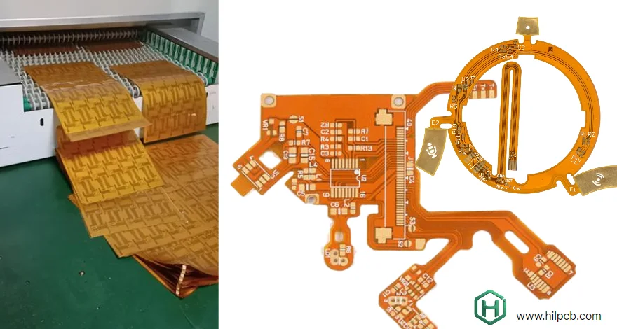
Flex fabrication commonly includes material preparation, imaging and etching, drilling where required, plating, coverlay lamination, surface finish, stiffener bonding, profiling, inspection, and electrical test. Material movement and thin-panel handling make registration, lamination pressure, adhesive flow, dimensional compensation, and tooling strategy important.
Flex PCB assembly adds another handling problem: an unsupported circuit can curl, stretch, wrinkle, or shift during printing, placement, and reflow. Production may use a process panel, carrier, fixture, vacuum support, temporary adhesive, or dedicated tooling. The correct method depends on outline, thickness, component distribution, reflow process, cleanliness, and acceptable handling marks.
Key assembly controls include:
- Keep components and solder joints outside dynamic bend zones unless the product has a validated construction for them.
- Support thin panels during solder-paste printing and placement; define tooling holes and panel rails with the assembler before release.
- Review stencil apertures and reflow profiles for uneven thermal mass, stiffener regions, bottom-terminated parts, and connector coplanarity.
- Control polyimide moisture using the laminate, component, storage, and assembly specifications; do not apply an arbitrary bake that can damage finishes or adhesives.
- Inspect visible joints with AOI and hidden terminations with risk-based X-ray, then perform electrical or functional tests designed for the assembly.
What flex PCB failures should testing prevent?
Test evidence should map to the released use case. A continuity test before shipment cannot reveal a conductor that opens only at the end of travel or after temperature exposure.
| Failure or symptom | Likely contributor | Prevention or evidence |
|---|---|---|
| Intermittent open during movement | Excess strain, small radius, ED copper, poor fixture alignment | Strain-aware layout and representative dynamic test with continuity monitoring |
| Trace crack near pad | Abrupt width change, weak anchoring, bend too close to termination | Teardrop/anchor review, transition keepout, cross-section or inspection |
| Via or barrel crack | Via placed in or near bend, thick stack, repeated deformation | Move vias to rigid/stiffened zone; post-stress electrical test |
| Coverlay crack or delamination | Opening edge in bend, poor lamination, incompatible material/process | Coverlay geometry review, peel/adhesion evidence, environmental cycling as required |
| Connector finger failure | Wrong final thickness, plating, stiffener, or insertion geometry | Connector drawing review, dimensional inspection, mating-cycle test |
| Impedance shift or link errors | Bend changes spacing, hatched plane not modeled, transition discontinuity | Coupon TDR, channel model, interface test in formed condition |
| Component or solder-joint fatigue | Component in moving zone, unsupported mass, repeated bending | Relocate or stiffen component area; cycling plus functional monitoring |
| Assembly misalignment | Curling, inadequate carrier, material movement | Panel/tooling review, SPI/AOI, first-article verification |
IPC-TM-650 method 2.4.3 addresses flexural endurance testing for flexible printed wiring materials. Product life still requires a fixture and acceptance plan that reproduce the circuit's motion, construction, and failure criteria.
How should medical and automotive flex circuits be specified?
Medical and automotive labels do not replace product requirements. Medical flex may need lot traceability, controlled materials, validated processes, cleanliness, sterilization compatibility, and change control. Patient-contacting or implantable use adds packaging, biocompatibility, hermeticity, toxicology, and product-level risk controls that a bare flex circuit does not establish.
ISO 13485 is a medical-device quality-management-system standard, while ISO 10993-1 addresses biological evaluation within a risk-management process. Neither makes an unencapsulated PCB automatically biocompatible or implantable. IEC 60601-1 and EMC collateral requirements apply at medical electrical equipment level when relevant.
Automotive programs may require IATF 16949 workflows, PPAP, approved materials, change notification, thermal/vibration qualification, traceability, and customer-specific requirements. The product owner should invoke the exact requirements on the drawing and purchase order.
Scope and responsibility. A PCB/PCBA supplier can build the released flex construction and provide agreed inspection, traceability, coupons, and production-test records. The product owner remains responsible for bend-life targets, mechanical integration, signal and thermal performance, sterilization or body-contact safety, automotive qualification, and final product certification.
What drives flexible PCB cost and lead time?
The main cost drivers are material type, layer count, panel utilization, outline nesting, coverlay openings, fine features, via structure, controlled impedance, stiffeners, selective plating, assembly tooling, test coupons, dynamic-life testing, traceability, and order quantity.
Optimize the whole assembly, not only the flex price. A flex or rigid-flex circuit may cost more than a small rigid PCB while removing connectors, cables, manual wiring, inspection points, and enclosure volume. It can also cost more overall when a simple harness would meet the requirement.
Prototype lead time depends on stocked material and whether the build needs custom stack-up engineering, tooling, impedance coupons, unusual stiffeners, selective finishes, assembly fixtures, or reliability testing. Do not promise a fixed 5–7-day delivery before the construction and evidence package are reviewed.
What belongs in a flexible PCB RFQ?
Fabrication and mechanical data
- Gerber, ODB++, or IPC-2581 data; drill/rout files; netlist; fabrication drawing; dimensioned outline; panel constraints; and revision list
- Layer stack with copper type and thickness, dielectric/adhesive/coverlay requirements, total thickness by zone, surface finish, and approved alternates
- Bend-zone drawing showing bend axis, direction, inside/outside copper, radius, angle, moving length, stiffener boundaries, and keepouts
- Stiffener material, thickness, adhesive, alignment, final ZIF thickness, connector specification, and exposed-finger plating
Motion, environment, and electrical requirements
- Static/service/dynamic classification plus cycle count, speed, stroke, radius, torsion, temperature, humidity, and mechanical load
- Controlled-impedance nets, tolerance, reference-plane or hatch geometry, coupon structure, and required TDR/S-parameter/interface evidence
- Operating/storage environment, thermal path, voltage/current, cleanliness, coating, sterilization or chemical exposure, and product safety boundaries
Assembly, quality, and test
- BOM, centroid, drawings, component height and keepout data, panel/carrier requirements, programming, and functional-test specification
- IPC class and revision, medical/automotive addenda or customer clauses, serialization, lot traceability, record retention, certificates, and change notification
- Electrical test, AOI/X-ray expectations, dimensional report, microsection or peel evidence, bend-test fixture and sample plan, acceptance limits, and failure disposition
Reference Standards and Scope
Confirm revisions and exact contractual applicability before release.
- IPC-2221 — generic printed board design
- IPC-2223E — sectional design standard for flexible/rigid-flexible printed boards
- IPC-6013E — qualification and performance specification for flexible/rigid-flexible printed boards
- IPC-6013EM — medical applications addendum to IPC-6013E
- IPC-4202 — flexible base dielectric materials
- IPC-4203 — adhesive-coated dielectric films and cover materials
- IPC-4204 — flexible metal-clad dielectric materials
- IPC-A-600 — acceptability of printed boards
- IPC J-STD-001 — requirements for soldered electrical and electronic assemblies
- IPC-A-610 — acceptability of electronic assemblies
- IPC-TM-650 2.4.3 — flexural endurance test method for flexible printed wiring materials
- ISO 13485 — quality management systems for medical devices
- ISO 10993-1 — biological evaluation of medical devices within risk management
Why manufacture flexible PCBs with HILPCB?
HILPCB supports flex PCB manufacturing, rigid-flex PCB, SMT assembly, and turnkey assembly within one DFM and production workflow.
Published flex capability ranges include one to four layers as standard and up to eight layers for reviewed builds, 75/75 µm standard and 50/50 µm advanced trace/space, 0.20 mm mechanical and 0.10 mm laser-drilled hole options, and impedance verification targets subject to the approved stack-up and coupon plan. These limits are not freely combinable; material, copper, thickness, outline, panel, bend requirement, and inspection scope determine the buildable result.
The useful first step is a bend-zone and stack-up review. HILPCB can check copper type, layer symmetry, conductor direction, via and pad keepouts, coverlay openings, stiffener transitions, ZIF geometry, panel support, assembly tooling, coupons, and test access before quotation.
FAQ
What is the minimum bend radius for a flexible PCB?
There is no universal value. Minimum radius depends on total thickness, layer count, copper type and thickness, material and adhesive, bend direction, cycle count, temperature, and motion. Define the use case, review IPC-2223 and fabricator guidance, then validate the released stack-up.
Is rolled-annealed copper always required?
RA copper is generally preferred for repeated dynamic bending. ED copper can be suitable for bend-to-install or low-cycle applications. Foil type alone does not guarantee life; the bend geometry, grain direction, stack-up, processing, and test profile also matter.
Should a flex PCB use a solid or cross-hatched ground plane?
A solid plane improves return continuity and shielding but adds stiffness. A cross-hatched plane can improve flexibility, while changing impedance, shielding, and current capacity. Choose from mechanical and electrical analysis and validate the actual hatch pattern.
Can components be placed in the bend area?
Avoid components and solder joints in an active dynamic bend. Put them on a rigid or stiffened zone and move the bend transition away from the stiffener edge. Exceptions require a product-specific construction and fatigue validation.
How is flexible PCB cycle life tested?
Use a fixture that reproduces bend radius, angle or stroke, frequency, temperature, orientation, and mechanical load. Monitor continuity or resistance during cycling and define failure thresholds, sample size, inspection, and post-test electrical or functional checks.
What files are needed for a flexible PCB quote?
Send fabrication data, netlist, stack-up, bend-zone drawing, copper and coverlay requirements, stiffener and connector details, motion profile, environment, impedance targets, IPC class, quantities, assembly files, and the required inspection and bend-test evidence.
Request a flexible PCB DFM review
Send HILPCB the preliminary stack-up, bend-zone drawing, connector and stiffener details, motion profile, electrical requirements, and test plan. The review will determine whether the design fits standard flex, multilayer flex, rigid-flex, or a simpler cable/interconnect—and remove avoidable bend, tooling, and qualification risks before fabrication.