
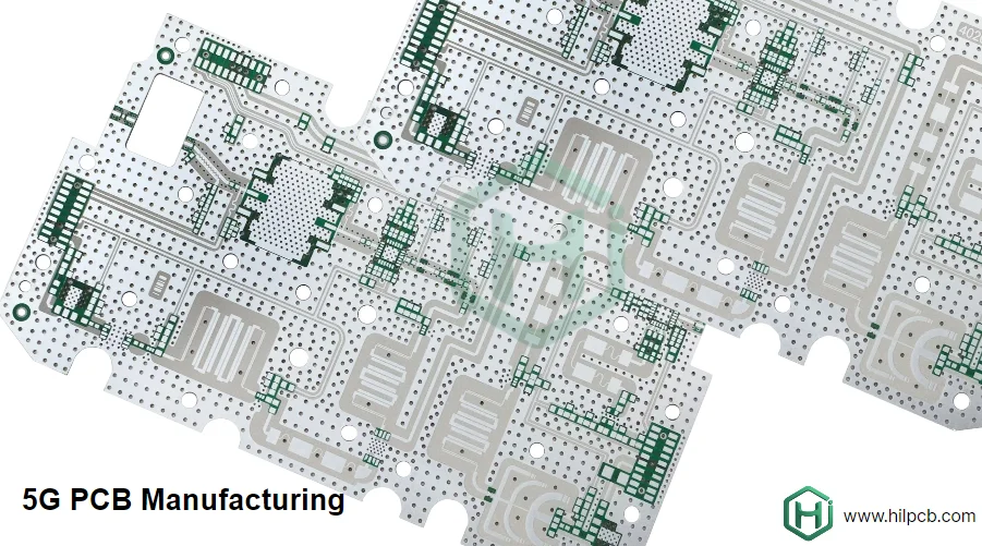
With the evolution of 5G toward 6G communication technology, operating frequencies have entered the millimeter-wave (mmWave) and even sub-terahertz (sub-THz) domains. This poses unprecedented challenges for PCBs carrying RF front-ends, baseband processing, and high-speed interconnects: lower transmission loss, stricter impedance control, and more complex heterogeneous integration. Against this backdrop, traditional testing methods struggle to meet the dual demands for precision and flexibility in R&D, prototyping, and small-batch production stages. Flying probe test technology, with its fixtureless and high-precision characteristics, has become a core means for verifying the electrical performance and signal integrity of these cutting-edge communication PCBs. It is not merely a simple continuity test, but a key tool for in-depth analysis of S-parameters, locating impedance mismatches, and verifying complex interconnects, providing indispensable assurance for the successful development of mmWave circuits.
Flying Probe Test vs. Traditional ICT/FCT: The Trade-off Between Flexibility and Precision
In the PCB testing field, In-Circuit Testing (ICT) and Functional Testing (FCT) are mainstream choices for the mass production stage, relying on expensive and long-development-cycle bed-of-nails fixtures. However, for 5G/6G prototype boards with fast iteration speeds and small batch sizes, this model appears inadequate.
The core advantage of Flying probe test lies in its "fixtureless" nature. It uses multiple independently movable probes, under precise software control, to directly contact test points, pads, or component pins on the PCB to perform electrical measurements. This approach brings several revolutionary advantages:
- Extreme Flexibility: Changing a test program is far faster and much cheaper than redesigning and manufacturing a physical fixture. This is crucial for high-frequency circuit R&D requiring frequent design modifications.
- Superior Access Capability: As component packaging (such as BGA, LGA) and routing density increase, the difficulty and space cost of reserving ICT test points for every net rise sharply. Flying probes can directly probe tiny pads or even Vias, solving the testability challenges of high-density designs.
- High-Precision Measurement: Flying probe test systems can integrate high-precision measurement instruments, such as Vector Network Analyzers (VNA), to directly perform S-parameter measurements on transmission lines, which is difficult for traditional ICT to achieve.
In contrast, the bed-of-nails based Fixture design (ICT/FCT) solution, while having an absolute advantage in single-board test speed, involves huge upfront investment and poor flexibility. Once the design changes, the entire fixture may be scrapped. Therefore, testing strategies should be prioritized differently at different stages of the product lifecycle: prioritize Flying probe test for in-depth verification and debugging during R&D and prototyping stages; shift to customized Fixture design (ICT/FCT) after entering mass production to pursue ultimate testing efficiency. Additionally, for complex digital logic parts, Boundary-Scan/JTAG testing can work synergistically with flying probe testing to achieve comprehensive coverage of digital interfaces and inter-chip interconnects.
De-embedding Methodology: Application Boundaries of TRL, LRM, and SOLT in Probe Testing
In the mmWave frequency band, any test equipment (including cables, adapters, and the probes themselves) introduces non-negligible parasitic effects, distorting the true Device Under Test (DUT) performance. To obtain accurate S-parameters of the DUT, "De-embedding" techniques must be used to strip the influence of these test systems from the measurement results. The accuracy of Flying probe test largely depends on the accuracy of the selected de-embedding method.
SOLT (Short-Open-Load-Thru): This is the most classic calibration method, relying on a set of precisely known standards (Short, Open, 50Ω Load, and Thru). Its principle is simple and widely applicable. However, realizing high-quality planar Open and Load standards on a probe station is extremely challenging, especially in the mmWave band, which limits its application in high-precision wafer or PCB level testing.
TRL (Thru-Reflect-Line): TRL calibration does not rely on ideal load standards but uses a Thru, a high-reflection standard (usually Open or Short), and a transmission line (Line) of known length. This method is very suitable for planar transmission line environments, such as microstrip lines and coplanar waveguides, making it the preferred choice for high-frequency Flying probe test. It can very accurately move the reference plane to the probe tip, thereby precisely extracting the performance of interconnect channels on the PCB.
LRM (Line-Reflect-Match): As a variant of TRL, LRM uses a transmission line, high reflection, and matched load as standards. It offers advantages over TRL in certain specific scenarios.
Which method to choose depends on the test frequency, substrate type, and available calibration standards. For high-frequency PCB requiring extreme precision, TRL calibration structures are usually designed specifically on the PCB to ensure the accuracy of de-embedding.
Comparison of De-embedding Calibration Methods
| Calibration Method | Core Advantages | Main Challenges | Flying Probe Applicability |
|---|---|---|---|
| SOLT | High versatility, industry standard | Planar standards (especially Open/Load) are not ideal in mmWave bands | Suitable for low-to-mid frequencies, limited precision at high frequencies |
| TRL | Extremely high precision in planar environments, no ideal load required | Requires precise Line standards fabricated on the DUT substrate | Best choice for mmWave PCB testing |
| LRM | Variant of TRL, insensitive to Line length requirements | Requires high-quality matched load standards | Preferred solution for specific application scenarios |
Probe Station and Fixture Design: Controlling Transition Effects and Ensuring Measurement Repeatability
A successful Flying probe test measurement depends not only on advanced VNAs and calibration algorithms but also on the mechanical precision of the probe station system and the quality of the "Transition" structure formed between the probe and the PCB pad.
Probe Selection and Transition Effects For mmWave signals, microwave probes in GSG (Ground-Signal-Ground) or GSSG (Ground-Signal-Signal-Ground) configurations are typically used. The tips of these probes are precisely designed to simulate the characteristic impedance of coaxial cables (usually 50Ω), thereby minimizing reflections at the contact point. However, the transition region from the probe tip to the PCB microstrip line or coplanar waveguide remains a major source of impedance discontinuity. The keys to controlling this region are:
- Probe Pressure Control: Excessive or insufficient pressure will affect contact stability and impedance matching. Modern flying probe systems feature closed-loop pressure control to ensure the Repeatability of every contact.
- Alignment Accuracy: The probe must land precisely on the center of the pad; any deviation will alter the electromagnetic field distribution in the transition zone, introducing measurement errors.
- Pad Design: Testability should be considered during the PCB design phase, designing pad patterns that match the probe configuration to achieve smooth impedance transitions.
Repeatability Control Measurement repeatability is a core metric for evaluating test system performance. In Flying probe test, this means that results should be highly consistent when the probe is lifted and lowered multiple times for measurement. This not only tests the mechanical stability of the probe station but is also closely related to the manufacturing quality of the PCB itself. For example, the flatness and thickness uniformity of surface finishes (such as ENIG, ENEPIG) directly affect the stability of contact resistance. Similarly, during the SMT assembly process, the printing quality of solder paste and the placement accuracy of components will also affect the electrical characteristics of the final test points.
S-Parameter Consistency Verification: Combined Effects of Bandwidth, Bias, and Temperature
For 5G/6G communication systems, passive interconnects (such as transmission lines, Vias, couplers) and active devices (such as amplifiers, switches) on the PCB must maintain consistent performance across wide bandwidths, different operating biases, and wide temperature ranges. Flying probe test provides an effective method to verify these performances on-board.
- Bandwidth Impact: 5G/6G signals have extremely wide bandwidths. S-parameter measurements must cover the entire range from low frequencies to the target operating frequency and even higher-order harmonics. This requires the test system (VNA, cables, probes) itself to possess sufficient Dynamic Range and bandwidth.
- Bias Network Integration: When testing active devices, DC bias needs to be provided without interfering with the RF signal path. This is typically achieved by integrating Bias Tees. In a flying probe test setup, how to cleanly introduce the bias network into the probe path is a technical detail requiring careful design.
- Temperature Impact: The dielectric constant (Dk) and dissipation factor (Df) of PCB materials change with temperature, directly affecting the impedance and loss of transmission lines. For high-speed PCB deployed in environments like outdoor base stations, performing S-parameter testing under high and low temperatures is crucial. This usually requires combining the probe station with a Thermal Chuck or thermal chamber to simulate the real operating environment.
mmWave PCB Performance Dashboard
Insertion Loss (S21)
-1.5 dB @ 40GHz
Target: < -1.8 dB
Return Loss (S11)
-25 dB @ 40GHz
Target: < -20 dB
Impedance TDR
50.2 Ω ± 1.5%
Target: 50 Ω ± 2%
Combining Optical and Electrical Testing: Synergistic Strategy of AOI/X-Ray and Flying Probe
The assurance system for a high-quality PCB product is multi-dimensional. Flying probe test excels at detecting deviations in electrical performance but cannot perceive their physical causes. Therefore, it must be combined with optical and X-ray inspection technologies to form a complete quality control closed loop.
- SPI/AOI/X-Ray inspection plays the role of a "sentry" in the production process. SPI (Solder Paste Inspection) ensures the quality of the "raw material" for soldering; AOI (Automated Optical Inspection) checks for missing, wrong, or reversed components and solder joint appearance after SMT assembly; X-Ray can penetrate components to inspect hidden defects such as voids and bridging in bottom solder joints of BGA, QFN, etc.
The value of this synergistic strategy lies in: when Flying probe test reports an open circuit on a certain net, AOI images might show that the component at that location is missing or has a dry joint. When flying probe testing discovers a short circuit between adjacent pins, X-Ray images might reveal that it is caused by solder balls or solder bridges under BGA balls. This rapid correlation from electrical phenomena to physical defects significantly shortens the cycle of fault diagnosis and process improvement. Whether it is complex SMT assembly or traditional THT/through-hole soldering, integrating these inspection methods is essential to ensure the high reliability of the final product. HILPCB's manufacturing process deeply integrates SPI/AOI/X-Ray inspection, providing a solid quality foundation for subsequent electrical testing.
Localization and Rectification of Consistency Failures: From S-Parameters to Physical Roots
When the S-parameter measurement results of Flying probe test fail to meet design specifications, the real challenge has just begun: how to quickly locate the root cause of the problem? This requires powerful analytical capabilities to correlate measurement data with physical structures.
Data Analysis Tools
- Smith Chart: It is the "stethoscope" for high-frequency engineers. By observing the trajectory of the S11 parameter on the Smith Chart, one can intuitively judge whether the impedance mismatch is capacitive or inductive, thereby inferring possible physical causes (e.g., Vias introducing extra inductance, pads introducing extra capacitance).
- Time Domain Reflectometry (TDR): By performing an Inverse Fourier Transform on frequency-domain S11 data, TDR results can be obtained, which display impedance changes along the transmission path like radar. If an impedance discontinuity occurs at a certain location, the TDR waveform will clearly show a peak or valley, the position of which directly corresponds to the fault point on the physical link, such as a connector, Via, or defective solder joint.
Root Cause Tracing and Rectification Once the approximate physical location of the fault is located via TDR, design files and physical inspection can be combined to determine the root cause.
- Design Issues: Incorrect transmission line width calculation, improper Via design (e.g., missing ground Vias), discontinuous reference planes, etc.
- Manufacturing Deviations: Over-etching or under-etching of circuits leading to line width changes, uneven dielectric layer thickness during lamination, etc. These issues are particularly critical for Rogers PCB using special materials.
- Assembly Defects: Poor soldering, such as dry joints leading to increased loss, or excessive solder changing pad capacitance. Whether it is SMT assembly or THT/through-hole soldering, process control is crucial.
HILPCB not only provides advanced testing services, but our engineering team can also assist customers in conducting in-depth failure analysis, providing comprehensive rectification suggestions from design optimization to process adjustment, ensuring that your prototype assembly project can iterate quickly and achieve success.
Key Points for Consistency Failure Rectification
- Data-Driven Decision Making: Fully utilize TDR and Smith Charts for precise localization to avoid blind guessing.
- Design-Manufacturing Synergy: Communicate closely with PCB manufacturers (such as HILPCB) to confirm whether manufacturing tolerances are within design limits.
- Focus on Transition Structures: Focus on checking all locations where impedance may change, such as connectors, Vias, and probe pads.
- Small Step Iterative Verification: After implementing rectifications, immediately verify through a new round of Flying probe test to form a rapid closed loop.
Conclusion
In the wave of rapid development of 5G/6G communication technology, PCBs have evolved from simple component carriers to key determinants of system performance. Flying probe test, with its unparalleled flexibility and high precision, has become a sharp weapon for mastering the challenges of mmWave and low-loss interconnects. It is not only a core tool for verifying designs, debugging prototypes, and ensuring small-batch production quality, but also a bridge connecting design, manufacturing, and assembly.
A successful test strategy requires the organic combination of Flying probe test with process control means such as SPI/AOI/X-Ray inspection, as well as Boundary-Scan/JTAG and Fixture design (ICT/FCT) in the mass production stage. Through precise de-embedding calibration, strict control of test system transition effects, and in-depth interpretation of S-parameter data, we can trace electrical performance issues back to their physical roots, thereby achieving efficient product iteration and optimization. HILPCB is committed to providing one-stop solutions from high-frequency PCB manufacturing to precision assembly and in-depth test verification, working with you to meet the challenges of future communication technologies and ensuring the perfect realization of your innovative designs.
Common Questions
Why is flying probe especially useful for 5G/6G prototype validation?
Because it avoids dedicated fixtures, adapts quickly through software, and can directly reach dense pads and vias in low-volume, fast-iteration development work.
Is flying probe limited to open and short testing?
No. When paired with instruments such as VNA or TDR, it can also support verification of impedance, insertion loss, return loss, and other key electrical behaviors.
What failures show up most often on mmWave PCBs?
Typical issues include discontinuities at vias and connectors, assembly-induced geometry shifts, excessive insertion loss, and impedance mismatch that worsens reflections.
Can flying probe replace AOI, X-ray, or ICT/FCT?
Not completely. It is best viewed as an early electrical-validation tool, while AOI and X-ray expose physical defects and ICT/FCT remains stronger for fixed, high-volume production testing.