
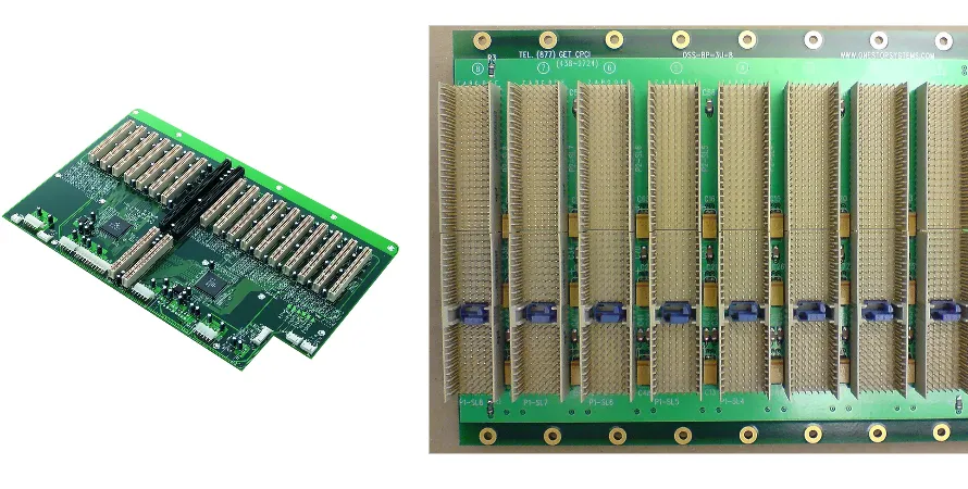
With the explosive growth of artificial intelligence (AI) and machine learning (ML), compute demand for AI servers is rising exponentially. As the “nervous system” connecting GPUs, CPUs, memory, and I/O modules, server backplane PCBs face unprecedented design and manufacturing pressure. In complex structures with dozens—or even over a hundred—layers, any tiny manufacturing defect can degrade performance or even bring the system down. That makes electrical integrity on every link non-negotiable. Among many test technologies, Flying probe test stands out as a critical method for validating AI server backplane PCB reliability thanks to its flexibility and precision.
This article explains the core principles of Flying probe test, why it is uniquely valuable for AI server backplane manufacturing, and how it supports signal integrity (SI), power integrity (PI), and advanced materials—serving as a practical AI server motherboard PCB guide to help you manage complex design and production challenges.
What is Flying Probe Test and how does it work?
Flying probe test is an automated, fixtureless PCB test method. Unlike traditional Bed-of-Nails testing that requires an expensive custom fixture for each PCB, a flying-probe machine uses 2–8 (or more) independently movable probes. Based on electrical-net data extracted from CAD/Gerber, it moves precisely to test points on the PCB (pads, vias, component pins) to take measurements.
The typical flow is:
- Data import: Import PCB CAD data (e.g., Gerber, ODB++) into the flying-probe system.
- Program generation: Automatically generate a test program and probe path to cover all nets efficiently.
- Automated test: Probes contact each test point and perform opens/shorts, resistance, capacitance, inductance, and even diode checks.
- Fault report: The system logs results in real time and outputs a detailed report with defect type and physical coordinates for rework or analysis.
The biggest advantage is being fixtureless—highly attractive for prototyping, low-volume builds, and High-Mix manufacturing.
Why do AI server backplane PCBs especially need Flying Probe Test?
AI server backplanes are far more complex than traditional PCBs. High layer count, high density, high speed, and high power make Flying probe test an essential quality gate.
- Extreme design complexity: AI backplanes often exceed 30 layers, include tens of thousands of connection points, dense BGA devices, and complex HDI structures. Building a traditional fixture can cost thousands to tens of thousands of dollars and takes time—too slow for rapid iteration.
- Fast NPI verification: AI hardware iterates quickly. Flying probe test needs no fixture lead time and can test immediately after fabrication, compressing design-to-validation cycles.
- Cost effectiveness at low-to-mid volume: AI backplanes are usually high-value, low-volume products. Fixture NRE amortized per board becomes painful. Flying probe test removes that upfront investment and supports AI server motherboard PCB cost optimization.
- Unmatched defect detection precision: Flying probes can touch almost any exposed conductive point and can cover 100% of electrical nets—catching subtle defects (high-resistance opens, latent short risks) that other methods may miss. For “zero-failure” server systems, this matters.
HILPCB AI server backplane manufacturing capability overview
| Technical parameter | HILPCB capability | Value for AI servers |
|---|---|---|
| Max layer count | 100+ layers | Supports ultra-large-scale, high-density routing demands. |
| High-speed materials | Megtron 6/7, Tachyon 100G, Rogers, etc. | Ensures SI for PCIe 5.0/6.0 and CXL links. |
| Min line/space | 2.5/2.5 mil (0.0635mm) | Enables high-density routing and complex BGA escape. |
| Max board thickness | 12mm | Meets thickness demands from high current and high layer count. |
| Impedance-control accuracy | ±5% | Protects high-speed differential-pair transmission quality. |
| Back-drilling (Back-drilling) | Depth control accuracy ±0.05mm | Eliminates via-stub reflections that degrade high-speed signals. |
How does Flying Probe Test protect high-speed signal integrity?
AI servers have entered the PCIe 5.0/6.0 and CXL era, with signaling rates reaching 32/64 GT/s. At these speeds, tiny impedance mismatches, crosstalk, or loss can cause bit errors. Flying probe test acts as an SI “guardian.”
It validates critical AI server motherboard PCB routing in several ways:
- Validate controlled impedance (indirectly): While impedance is mainly determined by design geometry and process control, flying probes can measure micro-resistance changes precisely via 4-wire Kelvin measurement—indirectly indicating impedance drift caused by etch non-uniformity or lamination issues.
- Detect differential-pair defects: For high-speed differential pairs, the test ensures there are no shorts between the pair and that safe electrical spacing to adjacent nets is maintained. It can catch weak shorts caused by copper debris or plating solution residues—often invisible to visual inspection.
- Ensure ground-network continuity: High-speed signals need stable, low-impedance return paths. Flying probes verify continuity across reference ground planes and help detect splits caused by drilling/lamination defects—critical for AI server motherboard PCB best practices.
Test strategy to improve power integrity (PI)
AI server GPUs and ASICs draw enormous power—single-board current can reach hundreds or even thousands of amps. A robust PDN is the foundation of stable operation. Flying probe test is equally important for validating PDN reliability.
- Detect power-to-ground shorts: One of the most common and dangerous defects. Flying probes can detect shorts between any power net and ground with 100% coverage before power-on, preventing instant destruction of expensive components.
- Verify continuity of high-current paths: For power planes and busbars carrying high current, testing confirms low resistance and continuity. End-to-end resistance measurement can reveal high-resistance points caused by poor interlayer connections (e.g., via voids), which would create voltage drop and local overheating under load.
- Isolate power domains: Complex backplanes include multiple separate power domains (12V, 48V, 3.3V, 1.8V, etc.). Flying probe test ensures these domains are correctly isolated and not accidentally shorted.
Key Flying Probe Test measurement parameters
- Opens (Opens): Check whether a net connection is broken to preserve signal-path integrity.
- Shorts (Shorts): Find unintended connections between different nets to prevent electrical failure.
- Resistance (Resistance): Measure net resistance precisely to identify high-resistance connections or potential fracture points.
- Capacitance (Capacitance): Measure inter-net capacitance to detect near-field shorts or wrong components.
- Inductance (Inductance): Verify inductance values of inductors or specific routing are within spec.
- Diode/transistor test: Basic functional verification for embedded passive/active elements on a bare board before assembly.
Test considerations for advanced materials and stack-ups
To meet low-loss requirements for high-speed signaling, AI backplanes widely use ultra-low-loss AI server motherboard PCB materials such as Megtron 6/7 and Tachyon 100G. These materials are expensive and demand strict process discipline.
- Early detection of material-related defects: Advanced laminates can suffer delamination or resin voids during lamination. While flying probes don’t “test the material” directly, these issues often cause electrical connectivity problems (e.g., via cracking) that flying probe tests will catch. Finding them before assembling expensive components prevents massive cost loss.
- Validate complex stack-up structures: Backplanes often use Sequential Lamination and Back-drilling. Flying probe tests can validate connectivity of newly added nets after each lamination step and ensure back-drilling doesn’t cut adjacent valid signal paths. For complex high-speed PCB programs, stepwise validation is essential.
- Monitor process stability: Analyzing flying-probe data across lots helps monitor process stability. For example, systematic resistance increases in a specific area can signal issues in plating or etching.
The role of Flying Probe Test in a DFM feedback loop
Flying probe test is not only a post-production quality gate—it is a bridge between design and manufacturing and a key part of a closed-loop DFM feedback system.
Test data provides valuable feedback to designers. For example, if reports show unusually high short rates in a certain region, it may indicate routing density beyond current process limits—violating AI server motherboard PCB routing best practices. Designers can use these concrete findings to increase spacing or optimize layout in the next revision.
As a leading PCB manufacturer, Highleap PCB Factory (HILPCB) integrates flying probe test deeply into our DFM services. We provide reports, analyze failure modes, and deliver actionable design-optimization recommendations to improve reliability and yield from the source.
Flying Probe Test execution flow
How to balance test coverage and cost?
Cost is a key factor in any manufacturing program. While 100% electrical test is mandatory for high-reliability products like AI backplanes, choosing the right strategy still matters for AI server motherboard PCB cost optimization.
- Prototype and low-volume phase: Flying probe test is the clear best choice. It avoids fixture NRE and long lead time, and offers maximum flexibility for design changes.
- Mid-volume production: As volume grows, trade-offs appear. Flying probe test has longer per-board time than Bed-of-Nails testing. Manufacturers must evaluate whether to parallelize with multiple flying-probe machines or invest in fixtures to accelerate test time. HILPCB provides cost-benefit analysis based on volume forecasts and product lifecycle.
- Hybrid strategy: In some cases, a hybrid approach makes sense: run flying probes for 100% opens/shorts, then use specialized TDR impedance tests on critical high-speed nets. This combines breadth (flying probe) and depth (dedicated instruments).
For high-value products like backplane PCB, investing in thorough early testing is far cheaper than discovering problems during system integration.
How HILPCB uses Flying Probe Test to improve AI backplane reliability
At HILPCB, Flying probe test is a cornerstone of our quality system—especially for complex AI server backplanes. We believe strong manufacturing capability must be paired with strict validation.
- Top-tier test equipment: We invest in high-speed multi-probe flying-probe testers with higher speed and accuracy, capable of handling 0.4mm BGA pitch and finer test points.
- Comprehensive coverage: We insist on 100% electrical test for AI backplanes and other high-reliability HDI PCB. Programs cover opens/shorts and parameter tests (resistance/capacitance) on critical nets to confirm electrical performance.
- Seamless handoff from fabrication to assembly: As a one-stop provider, our bare-board flying-probe results flow into our SMT assembly team. Only 100% qualified boards enter placement—eliminating assembly failures caused by board-level defects.
- Expert engineering support: Our engineers don’t just operate equipment—they interpret data. We collaborate closely with customers to analyze results and solve design/manufacturing issues, delivering the highest quality standards and reinforcing AI server motherboard PCB best practices.
Conclusion
In the AI compute race, AI server backplane PCB reliability is the foundation of system success. Flying probe test—with unmatched flexibility, precision, and cost effectiveness—is an ideal solution to meet these challenges. It is not only a production test tool; it is a quality hub that connects design, materials, and processes, ensuring complex routing and advanced material choices are realized accurately in the final product.
Choosing a partner like HILPCB—with advanced manufacturing capability and strict test workflows—is critical to building next-generation AI hardware. We deliver your innovation on the strongest physical foundation through craftsmanship and comprehensive quality control, including Flying probe test.
Common Questions
Why is flying probe test well suited to AI server backplane boards?
Because AI backplanes are high-value boards with complex routing, tight reliability demands, and frequent design optimization in early stages. Flying probe testing gives teams strong electrical coverage without waiting for custom fixtures, which is especially useful during prototypes and low-volume builds.
Why is 100% electrical test so important for AI backplanes?
A defect on a backplane can cause failures that are extremely expensive to debug once the full server is assembled. Testing every board helps prevent hidden opens, shorts, and net issues from reaching system integration or customer deployment.
Why might manufacturers combine flying probe test with other high-speed test methods?
Flying probe testing offers broad coverage, but some critical channels may still need deeper impedance or TDR-focused analysis. A hybrid approach lets teams screen the whole board efficiently while applying extra attention to the highest-risk nets.
How does flying probe test support cost control as volume changes?
It avoids fixture NRE and speeds up early validation when volumes are low, but manufacturers can later compare machine time, parallel capacity, and fixture investment as output grows. That makes it easier to choose the most economical test strategy at each production stage.