
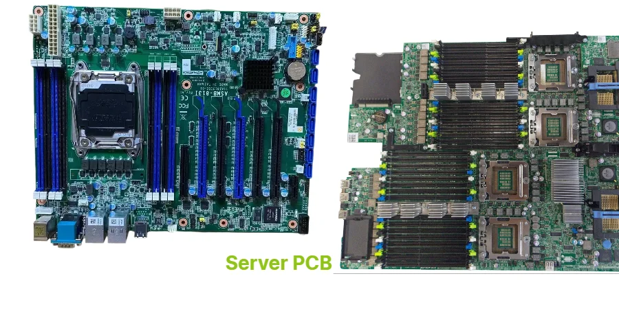
With the explosive growth of generative AI and large language models, data-center compute demand is rising faster than ever. GPU accelerators from NVIDIA, AMD, and others have crossed 1000 W per device, and full systems can reach tens of kilowatts. In this environment, internal bandwidth and power delivery reach a new scale. As the “nervous system” connecting compute, storage, and networking modules, the industrial-grade AI server motherboard PCB has become a key bottleneck for performance, stability, and long-term reliability. It is no longer just a component carrier—it is a complex engineering system integrating high-speed signaling, high-power distribution, and efficient thermal management.
As an engineer focused on high power-density solutions, I know every detail—from 48V VRM placement to PCIe 6.0 link implementation—directly affects AI cluster behavior. Traditional server PCB design assumptions no longer meet AI workloads. This article breaks down the core challenges of industrial-grade AI server motherboard PCB across design, fabrication, and assembly, and explains how advanced PCB technologies and manufacturing processes build a solid foundation for future AI compute. Highleap PCB Factory (HILPCB) has deep experience in this domain and provides one-stop support from design optimization to volume production.
Why is stackup design critical for AI server backplanes?
In AI servers, the Backplane or Motherboard carries massive data exchange between CPU, GPU, memory, and I/O modules. Once signaling moves into the PCIe 5.0/6.0 era (32/64 GT/s), the PCB’s electromagnetic behavior becomes a first-order factor. A well-designed AI server motherboard PCB stackup is the foundation for signal integrity (SI) and power integrity (PI).
The core goal is to provide a stable, continuous electromagnetic environment for high-speed differential pairs:
Ultra-low-loss material selection: Standard FR-4 has excessive dielectric loss (Df) at high frequency, causing severe attenuation. AI backplanes commonly use Ultra-Low Loss or Extremely-Low Loss laminates such as Panasonic Megtron 6/7/8 and Isola Tachyon 100G, keeping insertion loss low at 56/112 Gbps-class frequencies.
Reference-plane continuity: Every high-speed pair needs an adjacent, uninterrupted reference plane (GND) to provide a clean return path, stabilize impedance, and suppress EMI. In AI server motherboard PCB stackup planning, avoid routing across reference splits to prevent return-path discontinuities and noise injection.
Power/ground plane coupling: Tight coupling between PWR and GND planes forms inherent plane capacitance, enabling a low-impedance path for high-frequency current—critical for PDN stability.
Symmetry and warpage control: AI backplanes are large and often exceed 20 layers. Asymmetric stackups create lamination and reflow stress, driving warpage and hurting BGA solder reliability. Maintaining stackup symmetry is a basic manufacturing requirement.
How do you manage high-speed SI for PCIe 5.0/6.0?
When data rate doubles, SI problems can escalate dramatically. In PCIe 5.0 (32 GT/s) and above, every discontinuity—vias, connectors, BGA pads—can become a performance killer.
A systematic SI strategy includes:
- Tight impedance control: Tolerance often tightens from ±10% to ±7% or even ±5%. That demands precise etch/lamination control and strict AI server motherboard PCB testing using TDR.
- Via optimization: Through-hole vias introduce parasitic capacitance/inductance and create stubs that cause reflection and loss. Use Back-drilling to remove excess copper barrel, or use HDI Microvias and blind/buried vias to reduce discontinuities.
- Connector transition design: The region where signals enter high-speed connectors (e.g., MCIO, Gen-Z) is prone to impedance steps. Use EM simulation tools (Ansys HFSS, CST) to optimize pads, Anti-pads, and via fields for smoother transitions.
- Crosstalk suppression: As density rises, coupling increases. Increase spacing, use Stripline structures, and add Guard Vias in key regions to reduce near-end and far-end crosstalk.
For complex high-speed PCB projects, early DFM collaboration with an experienced manufacturer like HILPCB is a major success factor.
PCIe SI requirements vs. PCB design impact
| Parameter | PCIe 4.0 | PCIe 5.0 | PCIe 6.0 |
|---|---|---|---|
| Data rate | 16 GT/s | 32 GT/s | 64 GT/s (PAM4) |
| Nyquist frequency | 8 GHz | 16 GHz | 16 GHz (Baud Rate) |
| Total insertion-loss budget | ~28 dB @ 8 GHz | ~36 dB @ 16 GHz | ~32 dB @ 16 GHz |
| PCB material requirement | Mid/low loss | Low loss / ultra-low loss | Ultra-low loss / extremely-low loss |
What are the PDN challenges under a 48V architecture?
To handle kilowatt-class peak power for GPUs, AI servers are broadly migrating to 48V distribution. Compared to 12V systems, 48V reduces bus current by 4× and significantly cuts I²R losses. But it introduces new PDN design challenges for industrial-grade AI server motherboard PCB:
- High current density and hotspots: Even with lower bus current, regions near VRM and GPU devices still see very high current density. This drives the use of heavy copper (Heavy Copper), typically 3 oz to 6 oz (or more), to carry current and support heat spreading.
- PDN impedance control: AI load transients require hundreds of amps within nanoseconds. The PDN must stay ultra-low impedance across a wide bandwidth (DC to hundreds of MHz). This requires careful decoupling placement and a multi-stage network from bulk board caps to package-level high-frequency caps.
- VRM placement and efficiency: 48V-to-1V (or lower) conversion is a large step-down, tightening VRM efficiency and thermal constraints. VRMs should be as close to the load (GPU/CPU) as possible to minimize high-current path length and losses (PoL).
- Busbar integration: When current exceeds hundreds of amps, copper planes alone may not be sufficient. Integrating custom Busbars can provide ultra-low resistance/inductance current delivery, and can also serve as structural and thermal components.
How does thermal management handle kilowatt-level power?
Power becomes heat. When a PCB carries kilowatts, thermal management becomes a reliability lifeline. A strong industrial-grade AI server motherboard PCB must treat thermal design as a first-class constraint from day one.
- Build efficient thermal paths: Heat must be conducted away from hot components (VRM MOSFETs, inductors). Dense Thermal Vias under components can move heat into inner PWR/GND planes and spread it laterally across large copper areas.
- Embedded heat-spreading technologies: More advanced options include Copper Coin structures embedded in the PCB or using MCPCB. Copper Coins contact heat sources directly, providing low thermal resistance paths to the backside where heatsinks/cold plates can extract heat.
- System-level co-design: PCB thermal design must align with server cooling (air or liquid). In liquid cooling, layout must consider cold-plate channels and contact regions so key heat sources are covered.
- Thermal simulation: Use tools like Ansys Icepak early to predict temperature distribution and hotspots, then optimize placement and structures before costly re-spins—critical for reliable AI server motherboard PCB mass production.
Key thermal-management practices for AI server PCBs
- Prioritize heat paths: Minimize thermal resistance from hotspots to heatsinks; use Thermal Vias, large copper pours, and Copper Coin structures first.
- Optimize placement: Distribute high-power components to avoid clustered hotspots; consider airflow direction and place temperature-sensitive parts near cold-air inlets.
- Material selection: Within budget, select laminates with better thermal performance to improve overall heat handling.
- System integration: Coordinate PCB design with chassis airflow, heatsinks, and liquid-cooling modules to ensure heat is removed effectively.
- Simulation-driven design: Use thermal simulation before prototypes to catch and fix thermal risks early and shorten development cycles.
How do fabrication and assembly ensure final backplane performance?
Even the best design is only valuable if it can be manufactured and assembled accurately. Industrial-grade AI server motherboard PCB production places very high demands on suppliers.
On the fabrication side, key challenges include:
- Ultra-large size and high layer count: AI backplane PCB can reach 600 mm × 800 mm with 24+ layers, requiring large-scale lamination/plating/exposure equipment and excellent layer registration (often better than ±50 μm).
- Fine routing and drilling: To meet density, line/space moves into 3/3 mil (75/75 μm). Back-drill depth control, Microvia drilling quality, and via reliability directly affect SI.
- Material machining difficulty: Ultra-low-loss laminates can be harder and more brittle, requiring specialized drill/cut parameters to avoid rough hole walls and laminate cracking.
On the assembly side (SMT assembly), challenges are equally strict:
- High-density connector installation: Backplanes often carry many Press-fit connectors. Force and depth control are critical to long-term connection reliability.
- BGA soldering and inspection: Large BGAs (CPU/FPGA) demand precise reflow profiling to avoid opens/shorts or device damage. Because joints are hidden, 100% X-Ray inspection is often required.
- Board-level reliability (BLR): Large size/weight and complex assembly makes BLR a focus area, requiring stress/strain tests and thermal cycling to validate stability.
A capable partner like HILPCB can provide end-to-end support from PCB fabrication to SMT assembly, ensuring design intent is carried through the entire chain—critical for speed-to-market and consistent AI server motherboard PCB mass production.
How does a rigorous test flow protect industrial-grade reliability?
For data-center AI servers running critical workloads, reliability is non-negotiable. Comprehensive AI server motherboard PCB testing must span the full production flow:
- Incoming inspection (IQC): Strict checks of laminates, copper foil, chemistry, etc. to ensure key parameters (Dk/Df, Tg, CTE) match design requirements.
- In-process control (IPQC):
- AOI after inner-layer etch to detect shorts, opens, nicks, and defects.
- X-Ray inspection after lamination to verify inner-layer registration.
- Microsection analysis to verify plating quality, lamination build, and via structures.
- Final PCB test (FQC):
- E-Test (flying probe or fixture) for 100% open/short coverage.
- Impedance test (TDR) for all high-speed lines to verify characteristic impedance compliance.
- Reliability sampling such as thermal shock, solderability, ionic contamination, and more.
- Post-assembly test:
- ICT to validate soldering and basic electrical behavior.
- FCT to validate full board functionality in a realistic operating configuration.
With this end-to-end test chain, each shipped industrial-grade AI server motherboard PCB can deliver both performance and rock-solid reliability.
HILPCB capabilities for high-end AI server PCB manufacturing
| Item | Capability |
|---|---|
| Maximum layer count | 64 layers |
| Maximum board size | 800mm x 650mm |
| Minimum line/space | 2.5mil / 2.5mil |
| Maximum thickness | 10.0mm |
| Max aspect ratio (thickness/hole) | 20:1 |
| Impedance control tolerance | ±5% |
| Supported materials | Megtron 6/7, Tachyon 100G, Rogers, Teflon, etc. |
How do you achieve AI server backplane cost optimization?
Even with peak performance targets, cost is always a commercial reality. AI server motherboard PCB cost optimization is a system problem: it is not simply “cut manufacturing cost,” but optimize value across the full flow.
Design-stage cost control:
- Material trade-offs: Not every net needs the most expensive ultra-low-loss laminate. Use simulation to segment signals by speed and length, and mix material grades to balance performance and cost.
- Stackup optimization: With SI/PI constraints satisfied, reduce unnecessary layers. For example, optimizing routing can sometimes reduce a 24-layer design to 22 layers—significantly lowering cost. An optimized AI server motherboard PCB stackup is step one.
- DFM/DFA: Engage your PCB manufacturer and assembler early. Their process feedback prevents yield loss and rework caused by over-aggressive or incompatible design choices.
Manufacturing-stage cost control:
- Panel utilization: Good panelization increases laminate utilization and amortizes setup cost—especially in AI server motherboard PCB mass production.
- Process selection: Use Back-drilling only where needed; keep conventional vias for non-critical nets to reduce process cost.
Supply-chain coordination:
- Working with a supplier like HILPCB that provides PCB fabrication plus SMT assembly reduces communication and logistics overhead and improves cross-optimization, lowering total cost of ownership (TCO).
Why is choosing the right PCB manufacturer so important?
Industrial-grade AI server motherboard PCB design and production is a highly complex systems problem combining materials science, electromagnetics, thermals, and precision manufacturing. Selecting a manufacturer with strong technical depth, proven experience, and robust quality systems is a prerequisite for success.
An ideal partner should provide:
- Deep technical expertise to diagnose SI, PI, and thermal challenges and support DFM/DFA decisions.
- Advanced manufacturing capability for large size, high layer count, HDI, Back-drilling, Heavy Copper, and other complex builds.
- Strict quality control with end-to-end AI server motherboard PCB testing to ensure consistency and reliability.
- Flexible production and service across fast prototypes and high-volume builds, with one-stop PCB-to-PCBA delivery.
Highleap PCB Factory (HILPCB) fits this profile. We invest in advanced production and inspection equipment and maintain an experienced engineering team to help customers solve every critical issue in industrial-grade AI server motherboard PCB design and manufacturing.
Conclusion
The AI era is reshaping compute architectures at an unprecedented pace. In this transformation, the industrial-grade AI server motherboard PCB is an irreplaceable foundation. From PCIe 6.0 SI to kilowatt-class power and thermal control, and long-term reliability under harsh conditions, these challenges push PCB technology to new limits.
Building a high-performance AI server backplane requires tight coordination across design, fabrication, and assembly. With the right ultra-low-loss materials, optimized stackup planning, disciplined PDN and thermal design, and a partner with top-tier process capability and quality control, we can build the engines that will carry future AI compute.
If you’re looking for a reliable partner for AI server PCB challenges, contact HILPCB. Our experts provide full support from design optimization and material selection to volume manufacturing and assembly—helping you win in a competitive market.
Common Questions
Why do AI server motherboards need ultra-low-loss materials?
Because PCIe 5.0 and 6.0 channels run at data rates where standard FR-4 loss can consume too much of the signal budget. Ultra-low-loss laminates help preserve insertion loss margin across long links, connectors, vias, and large backplane structures.
What makes PDN design difficult on industrial-grade AI server boards?
AI servers combine extreme current demand, dense accelerator placement, and fast transient load behavior. The board must deliver stable power with low impedance while controlling heat, voltage drop, and mechanical stress across a very large multilayer structure.
Why is thermal design a PCB issue and not only a system issue in AI servers?
Because the PCB itself influences heat spreading, copper distribution, layer construction, and airflow interaction around high-power devices. Poor board-level thermal planning can undermine even strong system-level cooling hardware.
What should be validated before scaling an AI server motherboard PCB into production?
Teams should validate high-speed loss and impedance behavior, PDN stability, warpage control, connector transition quality, and assembly robustness around large BGAs and heavy power components. Prototype data is essential before committing to volume ramp.