
In today’s data centers, communication infrastructure, and HPC systems, power density is rising at an unprecedented pace. To keep up with compute demand, architectures are moving from traditional 12V to 48V—improving efficiency, but also raising the bar for PCB design and manufacturing in power-delivery and cooling systems. In this context, Low-void BGA reflow is no longer optional; it’s a cornerstone of long-term system stability. A seemingly small solder void can become a fatal weakness in a high-availability design—especially under high current and high heat-flux density on power devices.
As specialists in redundancy and hot-swap solutions, we know that excellent power systems depend not only on advanced circuit design, but also on flawless manufacturing execution. From complex 48V to 12V conversion board stackup planning, to following Digital VRM controller PCB best practices, to final reliable assembly—every step matters. This article explains why Low-void BGA reflow is so important, and how it works together with hot-swap control, redundant power, and PMBus monitoring to deliver high reliability and high availability in power and cooling systems.
The core value of Low-void BGA reflow: why voids are the “enemy” of reliable power
BGA packages, with high I/O density and strong electrical performance, have become the default for modern power ICs, FPGAs, and processors. But during reflow, flux volatiles or other contamination can be trapped inside molten solder, forming small bubbles—voids. For ordinary signal pins, small voids may be acceptable. For power and ground pins—especially large thermal pads under power devices—voids are the enemy of reliability.
Their impact shows up in three main ways:
- Worsened thermal conduction: Voids have very low thermal conductivity, effectively creating an “insulating layer” between the die and the PCB. This increases junction-to-board thermal resistance (Rth j-b), trapping heat in the device. Local hotspots accelerate aging, reduce performance, and can trigger thermal failures at peak load. For designs targeting maximum SiC rectifier board reliability, this is unacceptable.
- Reduced mechanical strength: Voids reduce the effective solder cross-section, weakening mechanical strength and fatigue resistance. Under temperature cycling, vibration, or mechanical shock, high-void joints crack more easily and can ultimately fail open.
- Lower current-carrying capability: On high-current pins, voids constrict current paths, increasing local current density. This creates extra I²R heating and can worsen electromigration risk, further increasing thermal-runaway probability.
That’s why processes such as vacuum reflow, optimized solder-paste chemistry, and precise profile control—i.e., Low-void BGA reflow—are used to keep voiding within IPC guidance (e.g., IPC-7095) at Class 3 levels (often <10%), forming the first line of defense for high-power-density PCB reliability.
48V architecture challenges: stackup design and thermal co-optimization
As data-center power architectures shift to 48V, 48V to 12V conversion board stackup becomes increasingly critical. These converter modules often use multi-phase buck topologies with controller/driver/power MOSFET integration and very high power density. Large thermal pads under BGA power-stage devices must carry tens of amps while dissipating tens of watts.
A successful 48V to 12V conversion board stackup must co-optimize electrical, thermal, and manufacturing factors:
- High-current path planning: Use Heavy Copper PCB to build wide power/ground planes on inner and outer layers, minimizing IR drop and parasitic inductance.
- Thermal design: Build dense arrays of thermal vias under BGA thermal pads and connect them directly to internal/bottom heat-spreading planes. These vias should be plated and filled to maximize thermal efficiency and ensure reliable solder fill.
- Material selection: Use high Tg materials to handle local high temperatures from power devices and maintain dimensional stability and reliability over long-term high-temperature operation.
But even great design needs perfect manufacturing to deliver results. If BGA solder joints have severe voiding, carefully designed thermal vias and heavy-copper layers can’t do their job—heat is trapped in the die and devices fail early. Low-void BGA reflow is therefore the key manufacturing step that unlocks the full potential of 48V to 12V conversion board stackup designs.
Standard reflow vs. Low-void BGA reflow: process comparison
| Metric | Standard reflow | Low-void BGA reflow (vacuum reflow) |
|---|---|---|
| Thermal-pad voiding | 15%–30% (or higher) | < 5% (typical), meets IPC Class 3 requirements |
| Junction-to-board thermal resistance (Rth j-b) | Higher; heat path is constrained | Significantly reduced; heat-dissipation efficiency maximized |
| Expected MTBF | Lower; more vulnerable to thermal stress | Much higher; improved system reliability |
| Typical applications | Low-power, non-critical designs | High power density: servers, communications, automotive electronics |
Manufacturing-precision requirements for Digital VRM controllers and PMBus monitoring
Modern power-delivery systems increasingly rely on sophisticated digital controllers. Designing according to Digital VRM controller PCB best practices enables accurate regulation, fast transient response, and flexible configuration. These digital VRM controllers often use high-pin-count BGA packages that integrate sensitive analog sensing, high-speed digital logic, and communication interfaces.
Solder-joint voiding affects these devices in two ways:
- Power integrity (PI): Voids on the controller’s power/ground pins add parasitic inductance and resistance, shifting PDN impedance and potentially destabilizing internal rails—reducing control accuracy.
- Signal integrity (SI): On high-speed interfaces (e.g., PMBus or SVID), voiding can slightly perturb path impedance. The effect is often smaller than on power pins, but under fast edges it can still increase reflections and jitter.
Closely related is PMBus monitor PCB manufacturing. PMBus (Power Management Bus) enables telemetry, alerts, and remote serviceability. Monitoring ICs report voltage/current/temperature and receive commands from system management controllers. If a monitoring IC fails due to BGA solder defects, the system loses its “eyes and ears”—making redundancy and hot-swap strategies far less effective.
High-quality PMBus monitor PCB manufacturing is therefore not just about component selection; it’s about ensuring absolute reliability at every interconnect. HILPCB uses strict AXI workflows, including 100% inspection of critical BGA devices, to keep voiding within the most demanding requirements—protecting long-term stability of the digital control and monitoring chain.
Reliability design in redundant and hot-swap systems: from OR-ing to current share
High-availability systems are built on redundancy and hot-swap. N+1 or N+N PSU architectures keep systems running continuously even if a single PSU fails.
- OR-ing: The key technique that allows parallel PSU outputs while preventing reverse current into a failed unit. Traditional diode OR-ing causes voltage drop and power loss, so modern designs often use MOSFET-based “ideal diode” controllers. Many of these controllers and MOSFETs use BGA/QFN packages with thermal pads—so solder quality directly determines reliability of the redundancy path.
- Hot-swap control: Hot-swap controllers manage inrush current on insertion/removal via soft-start and provide OCP/OVP/UVP. They are critical nodes in the system.
- Current share: Balances load across parallel modules to avoid overloading any single unit, improving lifetime and efficiency.
In these applications, any BGA defect on a key power path can collapse an entire redundancy strategy. For example, if a BGA joint on an ideal-diode MOSFET overheats and fails due to voiding, a redundancy path may open and the system can silently degrade into a non-redundant state. That’s why Redundant PSU backplane cost optimization cannot mean cutting manufacturing quality. True optimization reduces downtime losses by improving MTBF and reducing MTTR. With extensive experience producing Backplane PCB, HILPCB understands how directly backplane reliability impacts system availability.
Key reminders for designing low-void BGA joints
- Pad design: Follow best practices for Solder Mask Defined (SMD) or Non-Solder Mask Defined (NSMD) pads. For large thermal pads, use window-pane or grid stencil apertures to help flux volatiles escape.
- Via treatment: Via-in-Pad must use resin plugging and plated-over filled vias (POFV) to prevent solder wicking, which can cause voiding or insufficient solder volume.
- PCB surface finish: Prefer flat finishes such as ENIG or OSP to ensure consistent solder-paste printing.
- Work with your manufacturer early: Engage a manufacturer like HILPCB during early design to align on process capability and co-optimize DFM (Design for Manufacturability).
SiC power-device challenges and reliability validation
Wide-bandgap devices such as SiC are increasingly used in high-efficiency, high-frequency power conversion. SiC MOSFETs and diodes can operate at higher junction temperatures with faster switching and lower Rds(on). But this raises new assembly challenges and tighter requirements for SiC rectifier board reliability.
SiC’s benefits depend on efficient heat extraction. Heat-flux density is high, and any thermal bottleneck is amplified. Voids under BGA/QFN thermal pads become “traffic jams” in the thermal highway—pushing junction temperature far above expectation, eroding performance advantages and harming long-term reliability.
To ensure SiC rectifier board reliability, rigorous validation is required, such as:
- Accelerated life testing (ALT): Run under high temperature, humidity, and electrical stress to simulate aging across the product lifecycle.
- Temperature cycling test (TCT): Cycle between extreme temperatures to evaluate solder-joint fatigue under CTE mismatch.
- X-ray non-destructive inspection: 100% inspection after assembly for critical devices to quantify voiding and ensure compliance.
In practice, boards built with Low-void BGA reflow consistently outperform standard processes in these harsh tests, often improving MTBF by multiples.
Manufacturing and assembly: process control for Low-void BGA reflow
Reliability design must be realized in manufacturing and assembly. Achieving Low-void BGA reflow is not a single technique—it’s a system engineering effort across materials, equipment, and process control. As a leading PCB solution provider, HILPCB delivers top assembly quality through these key controls:
- High-quality solder paste and storage: Use low-void-optimized solder paste with controlled flux activity and volatility profiles, and strictly control storage temperature/humidity and shelf life for stable performance.
- Precision stencil design and printing: Design apertures for the BGA pad pattern; use laser cutting and electro-polishing for smooth, accurate apertures. Use high-accuracy automated printers and 3D SPI (Solder Paste Inspection) to ensure consistent paste height/volume/shape.
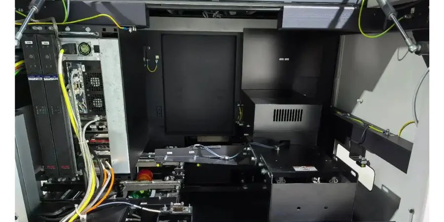
- Vacuum reflow equipment: The core enabler for low voiding. In the peak zone after solder melting, the oven chamber is evacuated to vacuum or near-vacuum. The pressure differential expands internal gas and drives it out, minimizing voids.
- Optimized reflow profiles: Customize ramp/soak/reflow/cool curves based on PCB thickness, layer count, copper area, and component thermal mass—ensuring proper heating while avoiding thermal shock.
- Strict AXI (X-ray) inspection: Use high-resolution 2.5D/3D X-ray equipment for non-destructive inspection of BGA/QFN bottom-terminated parts. Measure void area ratios to provide quantitative process validation and quality control.
By integrating these advanced capabilities, HILPCB’s Turnkey Assembly systematically solves BGA voiding and provides robust process assurance for Digital VRM controller PCB best practices and PMBus monitor PCB manufacturing.
HILPCB Low-void BGA reflow capabilities
- ✔Voiding control: Key thermal pads can be controlled stably below 5% voiding, meeting IPC-7095 Class 3.
- ✔Inspection: High-resolution 3D X-Ray capability enables detailed analysis of BGA/LGA/QFN solder quality.
- ✔Process support: Supports precision assembly down to 0.35mm pitch BGA, with vacuum reflow options.
- ✔DFM/DFA analysis: Professional manufacturability/assembly feasibility analysis before build to reduce soldering risk from the source.
Balancing cost and value: a new view on Redundant PSU backplane cost optimization
In development, cost control is always a key topic. Redundant PSU backplane cost optimization is often simplified to BOM and fabrication cost reduction. But for backplanes and PSU modules that sit on the system’s power lifeline, that view is incomplete—and potentially dangerous.
Real cost optimization should focus on total cost of ownership (TCO), including:
- Development and manufacturing cost: Initial BOM and processing cost.
- Operating cost: Power loss, cooling, and energy usage.
- Maintenance and failure cost: Often hidden but huge. A single server outage can cause business loss, data loss, and brand damage that far exceed the hardware’s value.
From a TCO perspective, investing in high-reliability manufacturing like Low-void BGA reflow does not increase cost—it reduces risk, achieving a higher level of Redundant PSU backplane cost optimization. With higher MTBF and lower field failure rates, a robust power system delivers longer uptime—its core value.
Choosing a partner like HILPCB that cares about process detail and quality control means you’re not just buying PCBs and assembly—you’re buying reliability insurance. We help customers find the best balance between performance, reliability, and cost, ensuring every investment translates into real system value.
Conclusion
As power-delivery and cooling systems move toward higher power density and higher reliability, Low-void BGA reflow plays an indispensable behind-the-scenes role. It directly influences thermal performance, mechanical robustness, and long-term electrical behavior. Whether it’s complex 48V to 12V conversion board stackup design, precisely controlled digital VRM systems, or absolute-reliability redundant power architectures—low-void soldering is a fundamental prerequisite for meeting design goals.
As your trusted partner, HILPCB provides advanced PCB manufacturing and assembly capabilities—and, as specialists in redundancy and hot-swap solutions, deeply understands your pursuit of extreme reliability. Through systematic process control and strict inspection, we embed the value of Low-void BGA reflow into every product we deliver, helping you confidently address high-power-density challenges and build stable, efficient, reliable power and cooling systems.
Common Questions
Why is low-void BGA reflow so valuable in power and cooling systems?
Power-dense boards depend on efficient thermal paths and mechanically sound solder joints under heavy electrical and thermal stress. Lower voiding improves heat flow away from critical devices and reduces the chance of early degradation in high-load conditions.
How can solder-joint voiding affect redundant power architectures?
If a thermally stressed BGA joint fails in an ideal-diode, controller, or monitoring path, a redundant system can quietly lose one of its intended protection paths. That means voiding is not just a workmanship issue but a direct reliability concern for uptime and fault tolerance.
What validation methods are commonly used for these assemblies?
Teams often use X-ray inspection, temperature cycling, accelerated life testing, and other reliability screening to confirm solder integrity and thermal behavior. These checks are especially important for SiC or other high-power devices that run with elevated junction stress.
Which process steps help achieve stable low-void results in production?
Good results usually come from low-void solder paste, controlled stencil design, vacuum reflow, tuned temperature profiles, and quantitative AXI or X-ray inspection. Consistency matters as much as peak capability when the goal is reliable field operation.