
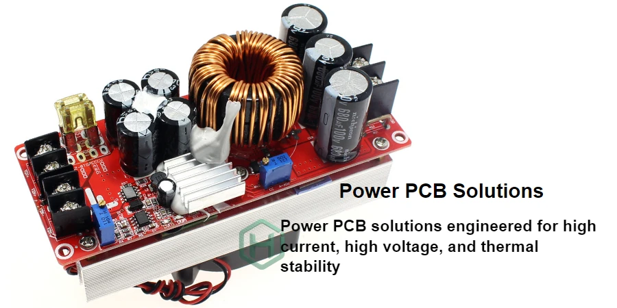
Across data centers, new-energy vehicles, 5G communications, and industrial automation, the relentless rise in power density and system efficiency is creating unprecedented challenges for power and cooling system PCB design. Under high current, strong vibration, and extreme temperatures, traditional soldering increasingly shows reliability and performance limits. In this context, Press-fit technology as a high-performance, solderless interconnect solution is becoming a preferred choice for engineers. By forming a gas-tight cold-weld joint through precision mechanical press-fit, it delivers outstanding electrical and thermal performance—and excels in mechanical stability and long-term reliability.
This article serves as a VRM/PDN design guide. We break down the fundamentals of Press-fit technology, and show how it works together with advanced PCB processes such as Heavy copper 3oz+ and HDI any-layer to optimize Power Integrity (PI) and Signal Integrity (SI)—helping you realize high-performance power and cooling system design and manufacturing with HILPCB.
Core advantages of Press-fit: why it stands out in PDN design
The heart of Press-fit technology is its unique connection mechanism. It uses a precisely designed “eye of the needle” pin or a solid compliant pin. When pressed into a precisely drilled and plated through-hole (PTH) on the PCB, the pin elastically or plastically deforms and applies a large, sustained normal force to the hole wall. This force creates intimate metal-to-metal contact, forming a gas-tight, cold-weld-like electrical connection. Compared with traditional soldering, the advantages are clear:
- Excellent electrical performance: Press-fit joints have extremely low and very stable contact resistance—typically at the micro-ohm level. In applications carrying hundreds of amps, this means lower I²R loss and less heat generation, directly improving PDN efficiency.
- No thermal-stress assembly: The process requires no heating, completely avoiding the thermal shock of soldering to PCB materials and components. This is especially important for thick-copper boards using Heavy copper 3oz+ or high-layer-count backplanes, which have high thermal mass and are difficult to solder—often risking warpage.
- Outstanding mechanical reliability: The strong normal force created by press-fit resists severe vibration, shock, and long-term thermal cycling. This rugged connection is critical in harsh environments such as automotive, aerospace, and industrial control—far superior to solder joints that may suffer cold joints or fatigue cracking.
- Simplified manufacturing and serviceability: Press-fit connectors are easier to install, remove, and replace, simplifying line assembly and field maintenance and significantly reducing total lifecycle cost.
PDN target impedance and modeling/simulation for Press-fit interconnects
In modern high-speed digital systems, maintaining a low and flat PDN impedance is essential for stable operation of core devices such as processors and FPGAs. The Target Impedance curve must be met across a wide band—from DC to hundreds of MHz and beyond. Press-fit technology plays a key role here.
Press-fit connectors inherently feature very low parasitic inductance (ESL) and parasitic resistance (ESR), making them an ideal low-impedance path from the VRM module to the load. In PDN modeling, engineers should use 3D electromagnetic simulation to extract an accurate S-parameter model of the press-fit pins and integrate it into the full PDN simulation chain. Results commonly show that, compared to equivalent soldered connections, press-fit can reduce PDN impedance peaks in the MHz band—improving transient response and reducing voltage noise.
To cover a wide frequency range, designs typically combine decoupling capacitors with different values and packages. Press-fit connectors provide low-inductance ground and power access points for these capacitors, ensuring they can deliver maximum effectiveness around their self-resonant frequency (SRF). A well-designed PDN paired with press-fit interconnects can reduce dependence on expensive high-performance capacitors and improve cost efficiency.
HILPCB capabilities: precision simulation and manufacturing
| Technical parameter | HILPCB capability | Value for Press-fit design |
|---|---|---|
| Press-fit finished-hole tolerance | ±0.05mm (50μm) | Ensures optimal normal force and long-term reliable electrical connection. |
| Barrel copper thickness | Average > 25μm | Provides sufficient mechanical strength to withstand insertion force and ensures a low-resistance path. |
| Supported copper weight | Up to 12oz | Fully supports Heavy copper 3oz+ designs for high-current transfer. |
| Simulation & DFM support | PDN impedance simulation and press-fit-hole design rule checks | Find and solve potential issues early to accelerate time-to-market. |
Combining advanced PCB processes: synergy between Press-fit, Heavy Copper, and HDI
The real power of Press-fit technology is that it integrates seamlessly with other advanced PCB manufacturing processes to build an ultra-high-performance power system.
First is the combination with Heavy copper 3oz+. In applications such as server power supplies and EV battery management systems (BMS), thick copper is a standard approach to carry high current and manage high heat. However, soldering thick copper layers is challenging: it requires high preheat, increases process difficulty, and risks component damage. Press-fit avoids this entirely. It can reliably connect to thick copper layers and efficiently conduct high current from the power plane into the connector pins. HILPCB has extensive experience in Heavy Copper PCB manufacturing, ensuring tight integration between thick copper and press-fit holes.
Second, in space-constrained high-density designs, HDI any-layer enables very high routing density through stacked microvias. Press-fit connectors can work alongside HDI any-layer structures to bring power directly out from inner power planes without consuming precious surface routing area—enabling better layer partitioning for power and signals and reducing coupling. In addition, Via-in-Pad plated over (VIPPO) places vias directly in pads and fills them with resin before plating over, further increasing routing density and thermal efficiency. In press-fit applications, nearby signal or low-current pins can use Via-in-Pad plated over (VIPPO) to achieve the most compact layout. HILPCB’s HDI PCB capability ensures robust microvia reliability for complex systems.
Thermal management and reliability: Press-fit performance in harsh environments
Thermal management is at the core of high-power system design. A press-fit joint is not only an electrical path—it is also an efficient thermal path. The metal pin makes tight contact with the plated hole wall, allowing heat from components to conduct quickly into large power/ground planes, which act as heat spreaders. In Heavy copper 3oz+ designs this effect is even more pronounced, lowering connector and nearby component temperatures and improving system reliability and lifetime.
On reliability, press-fit stands out even more. With no solder, solder-related failure modes are eliminated at the root: cold solder joints, voiding, Tin Whisker growth, and fatigue cracking under thermal cycling caused by coefficient of thermal expansion (CTE) mismatch. The gas-tight interface also helps prevent oxidation at the contact point in humid or corrosive environments, ensuring stable long-term electrical performance. Whether in vibration-intensive automotive electronics or decades-long-running communications Backplane PCB, Press-fit technology is an ideal choice for long-term reliability.
⚡ Press-fit: key points for high-performance interconnect and mechanical reliability
Completely eliminates secondary thermal shock from reflow or wave soldering. Protects High-layer count and thick-copper mainboards from delamination or pad-lift risk—ideal for high-precision, sensitive components.
Physical locking is achieved through strong normal force between the “eye-of-the-needle” pin and the hole wall. Under extreme automotive shock or continuous industrial vibration, joint robustness far exceeds traditional solder joints.
Prevents dry joints, cold joints, voids, and Tin Whisker growth at the process source. The cold-weld interface forms a gas-tight joint through molecular compression, effectively blocking oxide-layer formation.
Thanks to extremely high contact pressure in the press-fit zone, Contact Resistance remains highly consistent across repeated thermal cycling—preventing signal distortion or thermal-failure risk caused by poor contact.
Manufacturing and assembly considerations: ensuring long-term Press-fit reliability
Unlocking the full benefits of Press-fit technology requires precision PCB fabrication and strict assembly process control. Drilling and plating are the two most critical steps. The final finished-hole size must be controlled within a very tight tolerance (typically ±50μm) so that the pin generates the correct and uniform normal force after insertion. Barrel plating quality—including copper thickness and uniformity—directly impacts conductivity, heat conduction, and mechanical strength.
Surface finish selection is equally important. ENIG/ENEPIG/OSP are all viable finishes for press-fit holes. Among them, ENEPIG is often preferred for premium applications because of its excellent corrosion resistance and hardness, allowing it to better tolerate mechanical friction during insertion and deliver long-term reliability. OSP is a cost-effective option for cost-sensitive products.
During assembly, professional press-fit equipment is required, with real-time monitoring of insertion force, speed, and displacement. This ensures every pin is seated correctly—without PCB damage—while forming a reliable joint. HILPCB provides end-to-end services from DFM review to Turnkey Assembly. With strict process control—including meticulous handling of Via-in-Pad plated over (VIPPO) structures and rigorous Backdrill quality control—we ensure every press-fit connection meets the highest quality standards.
High-speed SI: co-optimizing Backdrill and Press-fit
While Press-fit is often used for power and low-speed signals, many modern connectors combine power and high-speed signals. In these cases, Signal Integrity (SI) becomes non-negotiable. The unused portion of a through-hole—the via “stub”—can behave like an antenna, causing reflections and resonances that lead to inter-symbol interference and data errors.
This is where Backdrill quality control matters. Backdrilling is a precision controlled-depth drilling process that removes excess stub from the opposite side of the PCB, minimizing reflections. For high-speed backplanes or motherboards using press-fit connectors, strict Backdrill quality control is key to SI: it can significantly improve eye opening and reduce bit error rate (BER).
Combining press-fit with HDI any-layer structures and backdrilling enables complex systems with excellent PI and SI. For example, power can be distributed efficiently via press-fit pins and thick copper, while high-speed signals use HDI any-layer microvias and backdrill-optimized paths for best overall system performance.
🏭 HILPCB assembly advantage: high precision and end-to-end reliability assurance
Integrates a Force-Displacement Monitoring system. By analyzing the insertion curve of each pin, hole-size anomalies and pin-deformation risks are rejected in real time—ensuring consistent gas-tight joints.
Breaks the barrier between PCB fabrication and assembly. We apply ultra-tight control of PTH finished-hole tolerance (+/- 0.05mm) and link it with MES for full digital traceability—from raw-material lots to press-fit force.
Strong in multi-process programs combining Press-fit + SMT + THT. With customized fixtures and staged reflow plans, we resolve assembly-stress challenges from high aspect ratio, thick copper boards, and multi-step HDI structures.
100% deployment of 3D AOI, 2D/3D X-Ray, and customized FCT. We inspect not only surface soldering quality, but also verify internal physical interconnect strength—ensuring IPC-A-610 Class 3 compliance.
Testing and validation: ensuring PDN performance from frequency domain to time domain
After design and manufacturing, thorough testing and validation of a press-fit-based PDN is the essential final step.
- Frequency-domain testing: Use a vector network analyzer (VNA) for 2-port measurement to precisely plot the PDN impedance curve (Bode Plot). By comparing measured results against simulation and Target Impedance, you can validate the design and confirm that press-fit connections deliver the expected low-inductance behavior.
- Time-domain testing: Use a dedicated load-step tool to emulate transient current demand changes (Load Transient), and a high-bandwidth oscilloscope to observe rail voltage droop (Vdroop) and recovery time. This directly evaluates dynamic PDN response under real operating conditions.
- Reliability testing: Run vibration, shock, and thermal-cycling environmental stress tests on assembled PCBs, and use four-wire measurements to track resistance change at press-fit joints—verifying stability and reliability under long-term use and harsh environments.
Common Questions
Why is press-fit technology a strong fit for power and cooling system PCBs?
Because it combines very low contact resistance and inductance with a solderless process that avoids thermal shock. In high-current, high-vibration, or high-thermal-mass designs, that combination improves electrical efficiency, mechanical robustness, and long-term reliability.
Which PCB details are most critical for reliable press-fit holes?
Finished-hole tolerance, barrel copper thickness, plating uniformity, and insertion alignment matter most. If those parameters drift, the pin may not generate the intended normal force, which can reduce retention strength and contact stability.
Can press-fit be combined with heavy copper, HDI, and backdrill features?
Yes. Heavy copper helps current transfer, HDI and VIPPO support routing density, and backdrill reduces high-speed stub effects. The key is co-designing the connector interface, stack-up, and manufacturing tolerances instead of treating each feature separately.
How should a press-fit PDN be validated after assembly?
Use frequency-domain impedance measurement with a VNA, time-domain load-step testing for Vdroop and recovery, and environmental reliability checks such as vibration and thermal cycling. Four-wire resistance tracking at the joints helps confirm that contact quality stays stable over time.
Conclusion
Press-fit technology is no longer just an alternative to soldering—it has become a cornerstone of modern high-performance power and cooling system design. By delivering unmatched electrical, thermal, and mechanical performance, it addresses the key challenges driven by high power density. When combined with advanced PCB processes such as Heavy copper 3oz+, HDI any-layer, Via-in-Pad plated over (VIPPO), and precision manufacturing practices like Backdrill quality control, the full potential of press-fit is further unlocked—enabling more efficient, more compact, and more reliable products.
At HILPCB, we understand the complexity of Press-fit technology and its strict requirements on manufacturing precision. With deep experience in advanced PCB fabrication and complex PCBA assembly, we can be the trusted partner that turns your most challenging design concepts into reliable products with exceptional performance.