
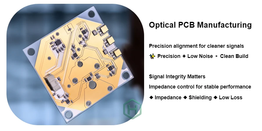
With the explosive growth of AI and ML, data-center east–west traffic is surging at an unprecedented pace. To meet the bandwidth demand of the 800G and even 1.6T era, QSFP-DD (Quad Small Form Factor Pluggable Double Density) optical modules have become a key interconnect solution. Behind their success is an extreme test of PCB technology. QSFP-DD module PCB mass production is no longer simple circuitry hosting—it is a complex system engineering problem that combines high-speed signal transmission, stringent thermal management, and precision opto-electrical integration. As the core substrate of opto-electrical interconnect, the PCB’s design and manufacturing quality directly determine module performance, reliability, and cost.
From the perspective of a CPO engineer, this article analyzes the core mass-production challenges of data-center QSFP-DD module PCB and presents an end-to-end technical playbook—from SI and thermal design, to material selection, assembly, and test—so you can successfully execute this high-difficulty manufacturing task.
High-speed signal integrity: the core challenges of QSFP-DD module PCB routing
In 800G QSFP-DD modules, 8 lanes of 112G/s PAM4 are commonly used. As the industry moves toward 1.6T, per-lane rates will rise to 224G/s. Such data rates bring unprecedented signal integrity (SI) challenges. Even small impedance mismatch, loss, or crosstalk can sharply degrade BER and ultimately break the link.
The first priority of QSFP-DD module PCB routing is loss control—both dielectric and conductor loss. To achieve this, engineers must:
- Select ultra-low-loss materials: traditional FR-4 is too lossy at high frequency. The industry widely adopts advanced low-Dk/low-Df materials such as Tachyon 100G and Megtron 6/7/8 to significantly reduce attenuation.
- Optimize differential routing: precisely control trace width/spacing and reference-plane spacing to achieve strict 100Ω impedance matching. Wider traces and smoother copper foils (HVLP/VLP) also help reduce conductor loss and skin effect.
- Refine via design: vias are major impedance discontinuities on high-speed paths. Use Back-drilling or HDI to remove via stubs and reduce reflections, and optimize Anti-pad geometry to reduce parasitic capacitance.
Crosstalk control is equally critical. In extremely compact layouts, high-speed channels sit very close. Increasing channel spacing, optimizing layer assignments, and adding Stitching Vias between adjacent lines can reduce NEXT and FEXT, keeping each channel’s Eye Diagram cleanly open. At HILPCB, we use advanced simulation tools to model every high-speed link and ensure our High-Speed PCB meets strict SI targets at the design stage.
Thermal management architecture: system-level cooling strategies for >20W modules
QSFP-DD module power has climbed from ~15W to >20W, and may approach 30W in the future. Concentrating this heat on a fingertip-sized PCB will overheat key devices (DSP, drivers, TIA) if not removed effectively—hurting performance and lifetime. Thermal management is therefore another lifeline of data-center QSFP-DD module PCB design.
An efficient thermal system is hierarchical, and the PCB is the key “thermal conduction hub”:
- Chip-level cooling: heat from high-power devices such as the DSP must first transfer through TIM into the module’s internal thermal structure.
- PCB-level conduction: the PCB must spread heat laterally and vertically around and under the chip. This is typically achieved with dense Thermal Vias, Heavy Copper PCB, or embedded Copper Coin. These reduce PCB thermal resistance and form efficient heat paths.
- Module-level cooling: heat is then conducted through the module housing to the front-panel riding heatsink, and removed by the system fan.
Design teams must accurately compute the module Thermal Budget and ensure Junction Temperature stays within safe limits under worst-case conditions. This requires tight co-design between PCB electrical design and the module’s mechanical/thermal architecture.
HILPCB manufacturing capability: advanced thermal-management PCB solutions
HILPCB focuses on high-challenge thermal-management PCB manufacturing. We offer end-to-end solutions to meet the cooling needs of high-power modules such as QSFP-DD:
- ✔ Embedded Copper Coin: embed solid copper directly into the PCB to create an ultra-low thermal-resistance path from chip to heatsink.
- ✔ Ultra-thick copper layers: manufacture copper up to 20oz to greatly increase current capacity and in-plane thermal spreading.
- ✔ High-thermal-conductivity via-fill resin: fill thermal vias with resin up to 8W/mK to build efficient vertical heat paths.
- ✔ High-thermal substrates: provide [High Thermal PCB](/products/high-thermal-pcb) to improve heat dissipation from the material level.
Power integrity (PDN) design: stable “blood supply” for critical chips
Power integrity (PDN) is the foundation of stable high-speed operation. In QSFP-DD modules, the DSP often runs below 1V but with very large transient current demand. A poor PDN causes IR Drop and excessive noise, directly degrading PAM4 signal quality and even triggering resets.
Successful QSFP-DD module PCB mass production requires a robust PDN, with the core goal of meeting Target Impedance:
- Low-impedance power path: use wide PWR/GND planes and ensure tight coupling to reduce inductance, providing a low-impedance return path for high-frequency current.
- Tiered decoupling capacitors: carefully place decaps near power pins. Bulk caps (tens to hundreds of μF) handle low-frequency energy, mid-value caps (nF to μF) handle mid-band transients, and small caps (pF to nF) filter high frequency—keeping PDN impedance low across the band.
- Co-simulation analysis: use PDN simulation tools to analyze the full path from VRM to the chip pads, predict ripple/noise, and optimize plane and capacitor placement accordingly.
Material selection and stackup design: balancing performance and QSFP-DD module PCB cost optimization
Materials are the foundation of PCB performance—and a major cost driver. In QSFP-DD modules, selection is a delicate trade among performance, reliability, and cost. The key to QSFP-DD module PCB cost optimization is an intelligent stackup strategy.
- Performance-driven: surface and inner layers carrying 112G/224G high-speed signals must use ultra-low-loss materials.
- Cost-aware: PWR/GND and low-speed signal layers can use lower-cost options such as high-speed FR-4 or mid-loss materials.
This Hybrid Stack-up approach controls total material cost without sacrificing critical channel performance. However, it adds manufacturing challenges (lamination compatibility, warpage due to CTE mismatch, etc.). Choosing an experienced manufacturer like HILPCB is critical—our mature hybrid-lamination process ensures reliable output.
In addition, Low CTE is critical for reliability. DSPs often use BGA packages; CTE mismatch between the PCB and the device creates stress during thermal cycling and can lead to solder fatigue. Selecting materials with CTE closer to the package can significantly improve long-term reliability.
High-speed PCB material performance comparison
| Material | Dk (10GHz) | Df (10GHz) | CTE (Z-axis, ppm/°C) | Application |
|---|---|---|---|---|
| Standard FR-4 | ~4.5 | ~0.020 | ~60 | Low-speed control signals, power planes |
| Mid-Loss (e.g., Isola FR408HR) | ~3.7 | ~0.011 | ~50 | 28G/56G NRZ signals, cost-sensitive designs |
| Low-Loss (e.g., Megtron 6) | ~3.3 | ~0.004 | ~40 | 56G/112G PAM4 signals, core high-speed channels |
| Ultra Low-Loss (e.g., Tachyon 100G) | ~3.0 | ~0.002 | ~30 | 224G PAM4 signals, long-reach backplane interconnect |
Manufacturability and assembly (DFM/DFA): ensuring yield for QSFP-DD module PCB assembly
A theoretically perfect PCB is worthless if it cannot be manufactured and assembled efficiently with high yield. For compact, component-dense QSFP-DD modules, DFM and DFA are especially important.
The core difficulty of QSFP-DD module PCB assembly is opto-electrical hybrid integration. Mounting the Optical Engine is the most precise and critical step in the entire flow.
- Precision alignment: the Fiber Array must align with waveguides on the PIC with sub-micron Alignment. This requires high-precision placement equipment and vision systems. Fiducial Marks on the PCB must be clear and accurately placed.
- Cure process: after alignment, UV or thermal Cure adhesive is used to fix the optical engine. Stress control during curing is critical; even tiny shifts can greatly reduce optical coupling efficiency.
- High-density SMT: beyond the optical engine, the PCB carries 0201 and even 01005 passives plus high-pin-count BGA/LGA devices. This demands very high placement accuracy and advanced soldering processes (e.g., vacuum reflow to reduce BGA voids) on the SMT Assembly line.
During the design phase, you must work closely with the PCB fab and assembly house to ensure pad design, solder mask openings, stencil apertures, and other details match process capability—paving the way for high-yield mass production.
Comprehensive test strategy: the critical role of QSFP-DD module PCB testing in mass production
Testing is the last—and most important—line of defense for product quality. For high-value QSFP-DD modules, a comprehensive strategy is essential, and QSFP-DD module PCB testing runs through every production stage.
- Bare-board test: after PCB fabrication, run 100% AOI plus flying-probe/fixture electrical tests to ensure no opens, shorts, or impedance anomalies.
- Post-assembly test: after PCBA, perform Boundary Scan and ICT to check solder quality and component functionality.
- Module-level functional test: the most critical stage. After installing the PCBA into the module housing, run full functional validation:
- BER Test: long-duration runs under various conditions (high/low temp, voltage corners) to ensure BER is below industry targets (e.g., 1E-12).
- Eye Diagram analysis: use high-speed oscilloscopes to capture PAM4 Eye Diagram and evaluate opening, linearity, and noise margin.
- CMIS compliance test: verify the management interface meets CMIS (Common Management Interface Specification) so the host can recognize and control the module correctly.
- Loopback: verify transmit/receive paths via internal or external Loopback.
Only after passing these stringent QSFP-DD module PCB testing steps can the product be qualified and shipped. For data-center QSFP-DD module PCB that must run 7x24, this is the reliability foundation.
💡 HILPCB: QSFP-DD module assembly and one-stop delivery matrix
Advanced lines tailored for optical modules, supporting ultra-high-density placement of 01005 components and 0.35mm Pitch BGA. For complex electrical/optical interface integration in QSFP-DD, we provide micron-level alignment accuracy assurance.
Deployed 3D-AOI, AXI (3D X-Ray), and high-frequency ICT/FCT testing. With strict electrical functional verification, every module meets zero-defect quality expectations in 800G+ bandwidth environments.
HILPCB engineering teams engage early and drive QSFP-DD module PCB cost optimization through DFM/DFA analysis. Combined with materials management, we offer a Turnkey one-stop service from prototype to volume production.
Conclusion
QSFP-DD module PCB mass production is an extremely challenging system engineering task that requires perfect balance across signals, power, thermal, and mechanical structure. From choosing the right ultra-low-loss materials, to refined QSFP-DD module PCB routing and PDN design; from a thermal solution co-designed with the module mechanics, to yield-focused QSFP-DD module PCB assembly and QSFP-DD module PCB testing—every step is technically demanding.
To succeed, you need not only deep design expertise but also a strong, experienced manufacturing partner. With years of focus on high-speed/high-frequency/high-reliability PCB fabrication and assembly, HILPCB provides end-to-end support from design optimization and material selection to final testing—helping you stand out in a competitive market and scale high-performance QSFP-DD optical modules into mass production.