
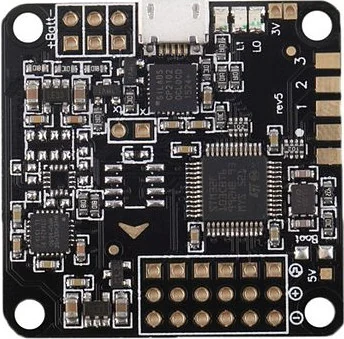
A quantum sensing PCB for UAVs is a board or carrier assembly that supports quantum-enabled sensors, precision timing references, or experimental inertial/navigation payloads inside a drone system. It should be reviewed as a low-noise, high-stability, size-weight-and-power constrained electronics platform, not as proof that a drone now contains a practical onboard quantum computer.
The original phrase Quantum Control PCB sounds futuristic, but a publishable engineering guide needs a stricter boundary. Today, the most defensible UAV connection is not a universal quantum flight-control board that instantly replaces classical control. It is a set of board-level design problems around quantum sensing payloads, GNSS-denied navigation support, timing stability, low-noise analog acquisition, vibration tolerance, EMI control, and careful integration with the ordinary flight-control stack.
Key Takeaways
- Quantum-enabled UAV electronics should be framed as sensor or payload support unless the project has specific quantum-computing hardware and cryogenic architecture already defined.
- A drone PCB cannot promise GPS-free centimeter accuracy, absolute communication security, or flight-safety certification by itself. Those outcomes depend on sensor physics, algorithms, mechanical integration, environmental testing, and system-level validation.
- The board-level work is still very demanding: low-noise front ends, stable references, rigid-flex packaging, vibration-resistant assembly, thermal control, shielding, and traceable PCBA testing.
- Cryogenic PCB and superconducting electronics belong to specialized research payloads or laboratory-adjacent systems, not ordinary commercial UAV flight controllers.
- For quote review, suppliers need the sensor type, SWaP limits, vibration profile, operating temperature, EMI constraints, connector strategy, test requirements, and any aviation or UAS assurance context.
In This Guide
- What a quantum sensing drone PCB is actually responsible for
- What quantum technology can and cannot claim in UAV electronics
- Architecture of a UAV quantum sensing payload board
- Low-noise sensor interfaces and timing stability
- SWaP, vibration, EMI, and thermal design
- Cryogenic and superconducting PCB boundaries
- Manufacturing, assembly, and validation controls
- Common failure modes
- Cost drivers
- RFQ checklist
- Why work with HILPCB
- FAQ
- References and standards
What a quantum sensing drone PCB is actually responsible for
A UAV quantum sensing board is best understood as a precision payload or navigation-support electronics assembly. It may interface with an atomic magnetometer, atomic clock, quantum inertial sensor, photonic sensing module, or other emerging sensor head. The PCB provides stable power, low-noise readout, clock distribution, shielded interconnect, data conversion, and communication to the flight computer.
That is a narrower but stronger claim than saying the board is a quantum flight controller. Most drones still rely on classical flight-control loops, IMUs, barometers, GNSS receivers, magnetometers, optical flow, visual-inertial odometry, LiDAR, radar altimeters, and onboard processors. A quantum sensor, when used, is more likely to supplement the navigation stack than replace the entire control system.
The main board-level question is therefore not “How do we put a quantum computer on a drone?” It is “How do we preserve the measurement stability of a sensitive sensor while the aircraft vibrates, radiates EMI, changes temperature, and fights for every gram of payload mass?”
| Review area | Board-level responsibility | What must stay system-level |
|---|---|---|
| Quantum sensing | Low-noise readout, stable biasing, shielding, temperature monitoring, sensor-head connection | Final navigation accuracy, drift model, fusion algorithm, calibration procedure |
| Flight control link | Deterministic data interface to autopilot or mission computer | Flight stability, obstacle avoidance, autonomous behavior, airworthiness claim |
| Secure communication | Hardware support for keys, secure boot, protected debug, RF isolation | Link security, cryptographic protocol approval, QKD deployment feasibility |
| Cryogenic support | Materials, interconnect, thermal sensors, low-outgassing or low-temperature design where required | Cryostat performance, superconducting sensor function, whole-payload thermal balance |
| Reliability | Assembly quality, vibration-resistant interconnect, traceability, inspection | Mission safety case, certification approval, operational compliance |
A strong drone quantum-sensing PCB review begins by deciding whether the board is a flight-control board, a navigation sensor carrier, a timing module, a payload controller, or a research instrumentation board. Each path has a different stackup, connector, inspection, and test-access burden.
What quantum technology can and cannot claim in UAV electronics
Quantum sensing is a real and active field for positioning, navigation, and timing. Cold-atom inertial sensors, atomic clocks, atomic magnetometers, and nitrogen-vacancy diamond sensors are being researched or developed as ways to improve navigation resilience when GNSS is jammed, spoofed, unavailable, or degraded. For UAV use, the practical value is strongest when quantum sensors are integrated into a hybrid navigation system rather than described as a complete standalone replacement.
Research direction should not be turned into guaranteed drone performance. A PCB should not be described as enabling millimeter-level GPS-free navigation, instantaneous decision-making, or absolute anti-jamming performance unless a specific product, sensor, test result, and system validation path support it.
The same boundary applies to quantum communication. Quantum key distribution can be valuable in some specialized communication architectures, but it is not a drop-in way to make all UAV control links “absolutely secure.” A UAV link still has practical constraints: optical alignment, range, weather, payload power, key management, authentication, radio coexistence, and mission architecture. For most UAV control electronics, the more immediate board-level security work is secure boot support, protected key storage, debug-port control, tamper-aware layout, RF coexistence planning, and robust conventional or post-quantum cryptographic implementation at system level.
Quantum computing needs an even stricter boundary. A drone-mounted superconducting quantum processor is not a realistic generic flight-control assumption. Superconducting quantum computing architectures typically require cryogenic environments and complex control/readout stacks. A PCB supplier can support low-temperature materials, impedance-controlled interconnect, flex/rigid-flex wiring, and precision assembly for research payloads, but it should not imply that ordinary UAVs can carry superconducting quantum computers as flight controllers.
Architecture of a UAV quantum sensing payload board
A practical UAV quantum sensing electronics stack usually includes the quantum or precision sensor head, a readout or excitation stage, local timing/reference circuitry, a processing or interface MCU/FPGA, power conditioning, and a data link to the flight computer. In some designs, the sensor head is physically separated from the electronics board to reduce heat, vibration, or magnetic interference.
The PCB architecture should be planned around signal quality before component density. Quantum-enabled sensors can produce weak signals, frequency-sensitive outputs, or measurements that drift if the local thermal, magnetic, or power environment changes. The board should not treat those signals like ordinary digital peripheral lines.
| Functional block | PCB design focus | Typical risk if ignored |
|---|---|---|
| Sensor-head interface | Shielded cable or flex connection, controlled grounding, connector retention | Noise pickup, intermittent contact, unstable calibration |
| Analog front end | Low-noise amplifiers, clean references, guard/shield structures where needed | Poor measurement resolution or drift |
| Timing/reference | Low-jitter clock distribution, thermal isolation, clean supply | Measurement instability and fusion errors |
| MCU/FPGA/data bridge | Deterministic interface to autopilot or mission computer | Latency jitter, packet loss, timing mismatch |
| Power conditioning | Separate low-noise analog rails, filtered digital rails, transient protection | Sensor noise, resets, false data during motor transients |
| Mechanical integration | Rigid-flex routing, strain relief, vibration control, mass balance | Connector fatigue, cracked solder joints, payload imbalance |
| Test access | Programming, boundary scan where applicable, calibration pads, logging | Slow bring-up and weak root-cause analysis |
A UAV layout often benefits from rigid-flex PCB when the sensor must be placed away from the processing board or aligned to the aircraft frame. Flex sections can reduce connector count and weight, but they add bend-radius, stiffener, impedance, and assembly controls that must be reviewed early.
For dense processing boards that include an FPGA, high-pin-count MCU, memory, RF transceiver, or miniaturized module, HDI PCB may be required. HDI should not be chosen only because the product sounds advanced. It should be selected when escape routing, layer count, controlled impedance, SWaP limits, or connector geometry justify it.
Low-noise sensor interfaces and timing stability
The most important design difference between a normal drone controller and a quantum sensing payload board is measurement discipline. Flight controllers can tolerate some digital noise as long as the IMU, power system, and radio remain within usable margins. Precision sensing boards often cannot. The analog chain, reference circuitry, and timing network must be protected from switching noise, motor noise, RF transmit bursts, and thermal gradients.
For a quantum magnetometer or other magnetic-field-sensitive payload, the board also has to avoid creating the error it is trying to measure. High-current traces, inductors, speakers, magnetic connectors, steel hardware, and switching regulators can all disturb the local magnetic field. The PCB review should therefore include a magnetic cleanliness check, not only an electrical DRC check.
For quantum inertial or timing payloads, phase noise, clock routing, and thermal drift may become the dominant issues. Reference oscillators should be placed away from heat sources and airflow shocks. Sensitive clock lines need controlled routing and low-noise supplies. When the board shares a bay with high-current ESC wiring, RF telemetry, or video transmission, cable routing becomes part of the electrical design.
| Design control | Why it matters | Practical PCB action |
|---|---|---|
| Separate analog and noisy power zones | Sensor readout can be corrupted by motor or RF noise | Place switching regulators away from low-noise inputs; use filtered rails and local LDOs where justified |
| Low-noise reference layout | ADC and timing errors can look like sensor drift | Keep references thermally stable, shielded, and close to the converter or timing IC |
| Guarded high-impedance nodes | Leakage and contamination can create bias errors | Use cleanliness control, coating strategy, guard structures, and test coupons when needed |
| Magnetic cleanliness | Current loops and ferromagnetic parts can distort measurements | Avoid high-current loops near magnetometers; document keepout around sensor head |
| Clock and sync integrity | Fusion algorithms depend on reliable time alignment | Use short, referenced clock paths and defined sync interfaces to the flight computer |
| Calibration memory | Field replacement needs traceable calibration data | Store sensor ID, calibration revision, and board serial number in nonvolatile memory or system database |
This is also where high-speed PCB and high-frequency PCB review may become relevant. Not every quantum sensing board is high-speed or RF-heavy, but UAV payload boards often include GNSS receivers, telemetry radios, video links, edge processors, or high-rate sensor interfaces that demand controlled stackup and clean reference planes.
SWaP, vibration, EMI, and thermal design
Drone electronics live under harsh size, weight, and power constraints. Adding a quantum sensor or precision navigation payload does not remove those constraints; it makes them harder. Every shield, connector, thermal pad, stiffener, and regulator has to justify its mass.
A good PCB review starts by separating what belongs on the aircraft from what belongs in a ground station or lab support system. If the sensor requires heavy optics, vacuum packaging, magnetic shielding, or cryogenic hardware, the board may be part of a research payload rather than a practical commercial UAV controller. That can still be a valid project, but the release package should say so clearly.
Vibration is a central reliability risk. UAV propellers, motors, and airframe resonances can fatigue solder joints, loosen connectors, distort sensor alignment, and create microphonic noise in sensitive analog circuits. The PCB should use appropriate mounting holes, keepout around screw stress zones, connector retention, adhesive or staking where specified, and component orientation that reflects the expected vibration axis.
EMI must be reviewed at system level. ESCs, DC-DC converters, telemetry radios, GNSS antennas, video transmitters, and payload processors can all interfere with a precision sensing board. The PCB can reduce risk through stackup planning, shielding, filtering, ground return control, cable entry filtering, and careful placement of radios and clocks. It cannot guarantee full aircraft EMC by itself.
Thermal design is equally important. A low-noise sensor board may not be high power, but it can still be temperature sensitive. A powerful edge processor or FPGA nearby may create gradients that cause measurement drift. The layout should keep heat sources away from reference and sensing circuitry, provide thermal paths for processors, and document any required airflow or enclosure assumptions.
| UAV constraint | Board-level response | Verification method |
|---|---|---|
| Low mass | Minimize connectors, use rigid-flex where it reduces harness weight, avoid unnecessary shield mass | Weight budget review and assembly drawing check |
| Vibration | Connector locking, via reliability, component staking, stiffeners, mounting-hole keepout | Vibration test, visual inspection, X-ray for hidden joints where needed |
| EMI | Shielding, filtering, partitioning, return-path control, cable-entry protection | Pre-compliance scan, conducted/radiated tests at system level |
| Thermal drift | Thermal separation between heat sources and references/sensors | Thermal imaging, chamber test, calibration drift tracking |
| Power transients | Brownout protection, rail sequencing, transient suppression | Power cycling, motor-load transient test, logging of resets and rail dips |
| Payload integration | Clear datum, connector direction, service access, strain relief | Mechanical fit check and harness pull/strain review |
Cryogenic and superconducting PCB boundaries
Cryogenic PCB design can be relevant to quantum research payloads, but it should not be presented as a normal UAV control-board requirement. Many superconducting quantum computing platforms require very low operating temperatures and dedicated cooling systems. That makes them fundamentally different from ordinary flight-control electronics.
A cryogenic PCB or interposer used in a research drone payload may need materials with predictable dielectric behavior at low temperature, low outgassing, controlled CTE mismatch, reliable plating, and mechanical compliance between warm and cold regions. Flex or semi-rigid coax transitions may matter more than a conventional FR-4 stackup.
Superconducting conductors also do not automatically improve drone endurance. The cooling system required to maintain superconductivity usually dominates the practical power, mass, volume, and complexity tradeoff. For UAV copy, it is safer to describe superconducting or cryogenic boards as specialized research support, not as a practical battery-life upgrade.
| Cryogenic topic | Safe PCB discussion | Avoid claiming |
|---|---|---|
| Low-temperature substrate | Material stability, CTE, copper adhesion, dielectric behavior | Universal suitability of one laminate for all cryogenic systems |
| Cryogenic interconnect | Cable/connector transition, thermal leak control, strain relief | Plug-and-play quantum processor connection |
| Superconducting device support | Research payload carrier, readout path, controlled impedance | Longer drone flight time from superconducting PCB traces |
| Thermal isolation | Warm/cold boundary, shielded harness, sensor thermal stabilization | Complete cryostat or cooling performance from PCB design alone |
| Assembly inspection | Cleanliness, X-ray, microsection, continuity at temperature where required | Full quantum-system performance proof |
For many UAV programs, the more practical route is not cryogenic quantum computing. It is improved GNSS-denied navigation through better IMU/GNSS/vision fusion, resilient timing, magnetometer discipline, high-quality sensor mounting, and possibly emerging quantum sensors where the payload budget and maturity allow.
Manufacturing, assembly, and validation controls
A quantum sensing UAV board should be built with a manufacturing plan that matches the sensitivity of the payload. The goal is not only electrical continuity. It is repeatable measurement behavior across boards, builds, temperatures, and vibration exposure.
The first manufacturing control is stackup stability. If the board carries high-speed sensor data, RF telemetry, or controlled-impedance timing lines, the stackup must define dielectric thickness, copper weight, material family, impedance targets, and reference planes before release. Late material substitution can shift RF behavior, clock performance, or calibration stability.
The second control is cleanliness. Flux residue, ionic contamination, moisture absorption, and coating defects can all become measurement errors or long-term leakage paths. This matters especially around high-impedance analog nodes, precision references, and exposed connectors used in field environments.
The third control is assembly visibility. QFN, LGA, BGA, MEMS modules, shield cans, and fine-pitch connectors need the right inspection chain. SPI controls solder paste. AOI catches placement and visible solder defects. X-ray is often needed for bottom-terminated components and hidden joints. Functional test should check not only power-on status, but noise floor, calibration readback, interface timing, and sensor-data stability where the customer provides fixtures or limits.
| Build stage | What to review | Typical evidence |
|---|---|---|
| DFM/DFT review | Stackup, impedance, panelization, test pads, coating keepouts, connector access | DFM report, stackup drawing, impedance coupon plan |
| Bare PCB fabrication | Material lot, copper thickness, drill quality, impedance, surface finish | Electrical test, TDR report, microsection where required |
| SMT assembly | Solder paste volume, placement accuracy, reflow profile, bottom-terminated components | SPI, AOI, X-ray, reflow profile record |
| Cleaning/coating | Ionic residue, coating coverage, connector masking, rework rules | Cleanliness report, coating inspection, traveler record |
| Functional test | Rail sequencing, noise, data interface, calibration memory, temperature sensors | Test log tied to board serial number |
| Environmental validation | Vibration, thermal cycling, humidity, power transient, EMI pre-scan | Project-specific validation report |
For prototypes and low-volume builds, prototype assembly can help teams iterate the sensor interface and mechanical integration quickly. For release builds, turnkey assembly becomes more useful when component sourcing, test fixtures, traceability, and coating/inspection requirements need to be controlled together.
Common failure modes
The hardest failures on drone precision-sensing boards are often intermittent. A board may pass a bench test and fail only after vibration, RF transmission, temperature shift, or motor-load transients. The release review should therefore focus on failure modes that can hide until integration.
| Failure mode | Likely cause | Board-level prevention |
|---|---|---|
| Sensor drift after takeoff | Heat from processor or regulator reaches the sensor or reference | Thermal separation, copper spreading for heat sources, calibration over temperature |
| GNSS-denied navigation support gives inconsistent data | Timing mismatch, vibration coupling, unstable sensor mounting | Sync line review, mechanical datum control, vibration test |
| Magnetometer or quantum magnetic sensor bias error | High-current loop, ferromagnetic hardware, nearby inductor or motor cable | Magnetic keepout, current-loop minimization, hardware material review |
| Random resets during throttle changes | ESC or battery transient couples into payload rail | Input filtering, rail sequencing, brownout logging, power transient test |
| RF link degrades sensor readout | Telemetry/video transmitter couples into analog front end | Shielding, RF keepout, cable routing, enclosure-level EMI review |
| Connector intermittent failure | Vibration, insufficient strain relief, non-locking connector | Locking connectors, staking, harness relief, pull and vibration testing |
| Coating-related leakage or rework damage | Poor masking, trapped contamination, inappropriate coating near connectors | Cleaning validation, coating keepout drawing, controlled rework instruction |
| Calibration mismatch after service | Sensor board, firmware, and calibration data not tied together | Serial-number traceability and stored calibration metadata |
The main lesson is that a high-end sensor does not rescue a weak PCB integration. Measurement quality depends on the whole chain: sensor physics, mechanical mounting, power quality, thermal conditions, EMI environment, firmware, and manufacturing repeatability.
Cost drivers
A quantum sensing drone PCB can become expensive quickly, but the cost drivers are not mysterious. They usually come from density, material selection, controlled impedance, rigid-flex construction, precision assembly, test time, and environmental validation.
| Cost driver | Why it raises cost | How to control it |
|---|---|---|
| Rigid-flex construction | More process steps, stiffeners, bend validation, lower panel utilization | Use flex only where it removes connectors or weight meaningfully |
| HDI and microvias | Sequential lamination and tighter drilling/registration | Use HDI only for true escape or miniaturization needs |
| Low-noise analog requirements | More layout separation, better references, shielding, cleaner supplies | Define noise targets early instead of overbuilding every rail |
| High-frequency/RF interfaces | Controlled stackup, impedance coupons, tighter material controls | Separate RF-critical routes from ordinary digital routes |
| Lightweight connectors | Specialized parts and mechanical validation | Freeze connector family before layout and assembly review |
| Coating or encapsulation | Masking, cure control, inspection, rework complexity | Apply only to exposed zones that need environmental protection |
| Environmental testing | Chamber, vibration, EMI, and fixture cost | Stage tests by prototype maturity and mission criticality |
| Traceability and calibration | Serialization, data capture, fixture integration | Decide what data must be tied to each board before build |
The cheapest path is usually not the lowest-layer board. It is the clearest architecture. A well-scoped rigid board, sensor cable, or small flex tail can cost less than an over-integrated “future-proof” board that tries to solve every research possibility at once.
RFQ checklist
For a useful quotation and DFM review, send enough information to separate a normal drone PCB from a precision quantum-sensing or navigation-support board.
Design files
- Gerber or ODB++ package
- IPC-356 netlist if available
- Stackup target and impedance requirements
- Pick-and-place file, BOM, and assembly drawing
- Flex bend drawing if using flex or rigid-flex
- Coating, potting, or keepout drawing if required
Sensor and system context
- Sensor type: atomic magnetometer, inertial sensor, timing module, photonic sensor, experimental cryogenic payload, or conventional IMU/GNSS sensor stack
- Required signal levels, bandwidth, noise limits, and reference stability
- Interface to flight computer: UART, SPI, I²C, CAN, Ethernet, USB, custom LVDS, or other protocol
- Calibration storage and serial-number traceability requirements
- Mechanical datum and sensor alignment requirements
UAV environment
- Payload mass and board outline limits
- Expected vibration profile or aircraft class
- Operating temperature and storage temperature
- Humidity, dust, salt fog, or conformal coating requirements
- Battery voltage range and motor/ESC transient assumptions
- Nearby RF systems, video transmitters, GNSS antennas, and telemetry links
Testing and quality
- Required inspection: SPI, AOI, X-ray, flying probe, ICT, functional test
- Noise-floor or sensor-stability test method, if available
- Vibration, thermal cycling, humidity, EMI pre-compliance, or chamber test requirements
- Serial-number, material-lot, and calibration-data traceability requirements
- Aviation, UAS, defense, or customer-specific documentation requirements
Why work with HILPCB
HILPCB supports UAV and precision electronics teams with PCB fabrication, assembly, and DFM feedback for compact, reliability-sensitive boards. For quantum sensing or experimental navigation payloads, the value is not in claiming that the PCB alone creates a quantum drone. The value is in protecting the measurement chain through better layout review, stackup control, assembly inspection, and test planning.
Relevant manufacturing routes include:
- HDI PCB for dense MCU/FPGA, sensor, and connector escape routing
- Rigid-flex PCB for lightweight sensor placement and reduced harness mass
- High-speed PCB for controlled digital, clock, and sensor-data interfaces
- High-frequency PCB for RF telemetry, GNSS-adjacent, or controlled RF structures
- Turnkey Assembly for BOM sourcing, SMT/THT assembly, inspection, coating coordination, and functional test handoff
Send the full design package and UAV environment assumptions through the Quote page or email [email protected]. The most useful early review is the one that catches sensor-noise, connector, vibration, coating, and test-access risks before the prototype absorbs them.
FAQ
Is a quantum control PCB a real replacement for a drone flight controller?
Not in the generic commercial sense. A safer description is that quantum-related PCB work supports specialized sensors, timing modules, or research payloads that may feed data into a classical flight-control or navigation system.
Can a quantum sensing PCB guarantee GPS-free centimeter navigation?
No. The PCB can support a sensor by providing stable power, low-noise readout, timing, and shielding. Final navigation accuracy depends on the sensor technology, calibration, mechanical integration, fusion algorithm, environment, and system-level validation.
Does quantum key distribution make a UAV command link absolutely secure?
No. QKD is a specialized communication architecture with practical constraints. UAV security still depends on authentication, key management, RF link design, firmware security, operational procedures, and system-level threat modeling.
Do drone quantum payloads always require cryogenic PCBs?
No. Some quantum sensing technologies may operate without cryogenic cooling, while superconducting quantum computing and some detectors require specialized low-temperature systems. Cryogenic PCB work should be treated as a research or mission-specific payload requirement.
Why are rigid-flex PCBs useful in drone sensor systems?
Rigid-flex designs can reduce connectors and harness mass while placing sensor heads at better mechanical locations. They also require bend-radius control, stiffeners, strain relief, and careful assembly inspection.
What is the most important RFQ information for this type of board?
The supplier needs the sensor type, signal/noise requirements, mechanical alignment needs, SWaP limits, vibration and temperature environment, connector strategy, coating requirements, and test plan.
References and standards
- RTCA DO-254 / EUROCAE ED-80 — Design Assurance Guidance for Airborne Electronic Hardware
- FAA AC 20-152A — Development Assurance for Airborne Electronic Hardware
- ISO 21384-3 — Unmanned aircraft systems / uncrewed aircraft systems operational procedures
- IPC-A-610 — Acceptability of Electronic Assemblies
- IPC-6012 — Qualification and Performance Specification for Rigid Printed Boards
- IPC-2221 — Generic Standard on Printed Board Design
- IPC-2223 — Sectional Design Standard for Flexible/Rigid-Flexible Printed Boards
- IEC 61000-4-2 — Electrostatic discharge immunity test
- IEC 61000-4-3 — Radiated radio-frequency electromagnetic field immunity test
- IEC 61000-4-4 — Electrical fast transient/burst immunity test
- IEC 61000-4-5 — Surge immunity test
- NIST post-quantum cryptography standards — system-level security migration context