
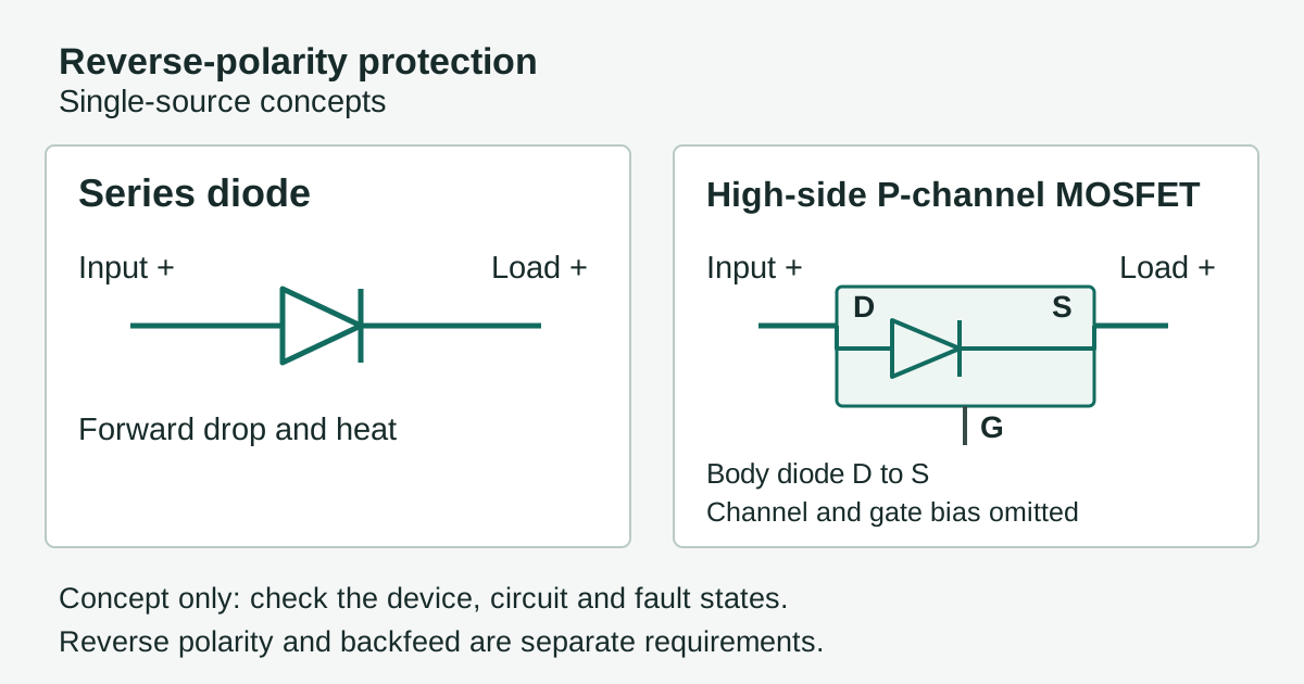
Choose a series diode when simplicity and low control overhead matter more than the voltage and power it loses. Choose a self-biased high-side P-channel MOSFET when the diode’s loss or voltage drop is unacceptable and the design can support the extra bias, transient and thermal analysis.
Neither choice automatically solves every input or output fault. The decision starts with the board’s actual voltage headroom, load current and operating states—not with a general preference for one semiconductor.
For example, a board used in reverse-light LED lighting may need protection against an incorrectly connected DC input while still delivering enough voltage to its load. The same tradeoff applies to other low-voltage boards: losing part of the supply across a diode may be inconsequential in one design and decisive in another.
Define the fault before choosing the component
Input polarity reversal means the supply is connected with the opposite polarity to that intended at the board input. A correctly implemented reverse-polarity protection stage is intended to prevent that mistake from applying damaging reverse voltage to the protected circuitry.
That is different from output-to-input reverse current: current flowing back toward the input from a charged output capacitor, a separately powered load or another energy source. This can occur even when nobody has reversed the input connector.
Also treat these as separate requirements:
- Overcurrent and short circuit: Excess current under a correctly polarized or faulted supply.
- Surge and transient protection: Control of voltage or energy excursions during connection, switching or external events.
- Isolation: Separation of circuits; a semiconductor that is off is not automatically a galvanic isolation barrier.
A fuse alone is not a reverse-polarity blocking component. It may be part of an overcurrent strategy, but it does not replace analysis of the polarity-protection path. Likewise, neither a diode nor a single MOSFET automatically supplies all the other protections.
Selection table: which tradeoff matters most?
| Design priority | Series diode | Self-biased high-side P-channel MOSFET |
|---|---|---|
| Minimum circuit complexity | Often the easier starting point: the main protection element needs no gate-control network. | Requires an intentional gate-bias arrangement and review of any associated clamp or bias components. |
| Tight voltage headroom | Forward drop reduces the voltage available to the board. Check it at the actual current and temperature. | An enhanced device may have a smaller conduction drop, but only with adequate gate drive and an appropriate resistance at temperature. |
| Conduction loss | Approximately load current multiplied by actual forward voltage. | Approximately current squared multiplied by actual on-resistance, provided the device is sufficiently enhanced. |
| Low available supply voltage | Straightforward behavior, but the drop may prevent startup or reduce load performance. | The available supply may not provide enough gate drive for the desired resistance; threshold voltage alone does not prove otherwise. |
| Charged or separately powered output | A correctly placed diode in the main path normally opposes output-to-input current, within its limits. Other paths still need review. | A single enhanced MOSFET does not itself guarantee reverse-current blocking. Its state depends on the circuit and terminal voltages. |
| Review and procurement effort | Check the diode’s electrical, thermal and package data along with its application conditions. | Check the MOSFET and the whole bias arrangement, including tolerances, startup, transients and thermal behavior. |
The simpler choice is not necessarily the lower-risk choice if its voltage drop leaves inadequate operating margin. Conversely, a lower calculated MOSFET conduction loss does not make the MOSFET the better choice if the board cannot drive it adequately or cannot verify its behavior in important fault states.
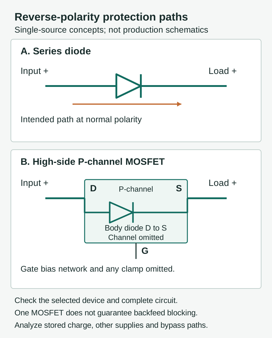
These are single-source concepts, not complete schematics. The MOSFET channel and gate-bias network are omitted; the actual circuit must establish suitable gate bias and may require a clamp. A single MOSFET does not guarantee output-to-input reverse-current blocking. Check stored charge, other supplies and bypass paths separately.
What the diode costs in headroom and heat
A series diode intentionally puts a forward voltage drop in the supply path during normal operation. The protected board therefore receives less voltage than the input provides, before allowing for connector, trace and other losses.
For steady conduction, approximate diode dissipation as:
P = I x VF
Use the forward voltage at the actual current and junction temperature, including relevant part variation. A convenient headline value from a data sheet may not represent the operating point. The resulting dissipation must be considered with the package, copper area, enclosure, airflow and surrounding heat sources.
The forward drop also changes the board-level decision. Check whether the downstream regulator, processor, LEDs or other load can start and operate at the lowest voltage they may actually receive. Startup current can differ from steady load current, so an acceptable steady-state calculation alone is not enough.
In the intended single-source path, a properly selected and connected diode normally opposes current when the input polarity is reversed. That expectation depends on the diode staying within its applicable limits and on there being no other path that bypasses it. Leakage, reverse voltage, transient behavior and thermal conditions still need evidence. For simple single-source examples, see Texas Instruments SLVA139, Reverse Current/Battery Protection Circuits.
What the self-biased MOSFET adds
The self-biased high-side P-channel MOSFET uses the circuit’s own terminal voltages to establish gate bias rather than relying on a separate actively commanded controller. When it is adequately enhanced in normal operation, approximate its steady conduction loss as:
P = I² x RDS(on)
The important resistance is the value applicable to the actual gate drive and junction temperature, with tolerances considered. An attractive on-resistance quoted under a gate-drive condition the board cannot provide is not a valid estimate for that board.
In particular, VGS(th) at its specified test current is not an adequate enhancement criterion. It identifies a threshold condition under the data-sheet test, not the gate drive needed to carry the board’s load at the desired low resistance. Review the applicable resistance curves or specifications over the expected operating range.
The topology also has control overhead. Depending on the exact design, gate-bias components and a gate-to-source clamp may be needed to establish or limit voltages. Their tolerances, leakage and behavior during startup and transients affect the result. Gate-source and drain-source limits, as well as transient and thermal safe operating area, require the exact component data and circuit analysis.
The intrinsic body diode matters during changes of state. It can provide a startup conduction path in an appropriate implementation, but its presence also means that the MOSFET cannot be treated as an ideal, symmetric switch. Check source/drain orientation against the selected device’s symbol and manufacturer datasheet; reversing the MOSFET’s orientation reverses the body-diode direction. The MOSFET symbol and pin-mapping check covers the separate step of verifying the symbol, footprint and physical part. Do not infer fault behavior from a generic symbol or from the steady-state loss calculation. For discussion of the P-channel topology and gate clamping, see onsemi AND90146, MOSFET Selection for Reverse Polarity Protection.
Fictional conduction comparison
For arithmetic only, assume a steady load of 1 A. At the stated operating conditions, suppose a diode has a hypothetical 0.4 V forward drop and a sufficiently enhanced MOSFET has a hypothetical 0.05 ohm on-resistance:
- Diode: 1 A x 0.4 V = 0.4 W
- MOSFET: (1 A)² x 0.05 ohm = 0.05 W
These are not part specifications, a thermal prediction, a real test, a lifetime estimate or a universal recommendation. Actual temperature, load transients, gate drive and tolerances change the result. Even with lower steady conduction loss, the MOSFET design still needs evidence for startup, faults and thermal behavior.
Operating-state evidence matrix
The expected behaviors below describe the intended main path, not a guarantee for every board. “Check” means to establish the result independently for the exact schematic, components and operating conditions.
| State | Series diode: expectation and evidence | Self-biased P-channel MOSFET: expectation and evidence |
|---|---|---|
| Normal startup | Expected: Current can reach the load after the input provides enough voltage to forward-bias the diode. Check: Startup current, diode drop, load voltage, ramp behavior and downstream startup requirements. | Expected: The bias arrangement should move the device into its intended conducting state; the intrinsic diode may participate during startup. Check: Gate and terminal voltage waveforms, load inrush, enhancement, device stress and startup with component tolerances. |
| Normal load | Expected: The diode conducts with a forward drop. Check: Minimum load voltage and dissipation over current, temperature and component variation. | Expected: An adequately enhanced device conducts with a resistive drop. Check: Actual gate drive, on-resistance at junction temperature, dissipation and thermal margin. |
| Reversed input | Expected: A correctly implemented diode opposes reverse current in the main path. Check: Applied reverse voltage, leakage, transients, component limits and any alternate paths. | Expected: The bias arrangement should keep the main path from applying damaging reversed input to the load. Check: Actual terminal voltages, gate-source and drain-source limits, body-diode effects, transient behavior and alternate paths. |
| Input collapse with stored output charge | Expected: The diode normally opposes discharge from the output back into the input through the main diode path. Check: Reverse stress, leakage, transient voltages and all other discharge routes. | Expected: The output charge can alter terminal and gate voltages; the single MOSFET may conduct back toward the input. Check: The time-dependent gate bias, current path, discharge current and device stress. Do not assume blocking. |
| Separately powered output | Expected: The main diode path normally opposes current from the powered output toward the input. Check: Voltage differences, leakage, reverse ratings and routes through other circuitry. | Expected: Behavior depends on how the independent output supply changes the MOSFET’s terminal voltages and bias. Check: Both supply sequences, possible backfeed, gate stress and conduction paths. |
| External bypass paths | Expected: The diode controls only the path in which it is installed. Check: Returns, signal connections, shields and connected equipment for paths around it. | Expected: The MOSFET controls only its intended path. Check: The same external paths, including paths that change gate bias or back-power the load. |
A simple single-source example cannot establish safe behavior for the last three states. If the product can be connected to another supply, a programmer, a communication cable or grounded equipment, include those connections in the circuit analysis rather than assuming the protection device sees the fault alone.
Turn the comparison into a design decision
Start with the diode if the board has comfortable voltage and thermal margin and a straightforward supply arrangement. Check the worst relevant forward drop against the minimum voltage needed by the load, then verify dissipation and reverse stress. Its lack of a gate network can make the evidence and component list easier to manage.
Move to the self-biased P-channel MOSFET when the diode’s headroom or dissipation is incompatible with the requirements. Then verify that the available gate drive produces acceptable conduction resistance across the operating range. Review the complete bias circuit, not just the MOSFET MPN.
For either choice, assess the transitions between states. Connection, disconnection, input collapse, load inrush and external transients can create conditions that a steady-state power calculation does not cover. A clamp, where used, also has tolerances and transient behavior; its presence is not proof that the semiconductor remains within its limits.
If output-to-input blocking is a requirement, state it separately and verify it separately. An enhanced single MOSFET can conduct in a reverse-current situation, while a diode’s main-path blocking does not account for bypasses or every possible voltage stress. The appropriate overall protection approach depends on the defined fault and system connections.
For context on how the protection parts fit alongside the rest of the board, see circuit board components.
Engineering, quality and procurement handoff
A useful handoff records the basis for the choice, not just “diode” or “P-channel MOSFET.” Include:
- Exact input conditions: Intended polarity, operating voltage range, source characteristics, ramp and collapse behavior, expected transients and fault duration.
- Exact load conditions: Startup and steady current, operating modes, output capacitance, separately powered states and minimum acceptable load voltage.
- System connections: Alternate returns, signal paths, external equipment and any circumstances in which the output can retain or receive energy.
- Controlled design: Schematic revision, layout or thermal assumptions, chosen MPN and package, and MPNs and tolerances for associated bias or clamp parts where applicable.
- Evidence: Relevant component data, calculations, state-by-state circuit analysis and the planned or completed verification evidence appropriate to the project.
- Acceptance criteria: Required behavior and allowable limits for each defined operating and fault state, including what constitutes a pass or failure.
Quality and procurement should know which assumptions and approved component identities the evidence depends on. A substitution can change forward voltage, on-resistance, leakage, gate behavior or thermal performance and should be evaluated against the same criteria. The component substitution approval checklist describes how to document and authorize an exact alternate for the relevant project scope.
HILPCB supports PCB manufacturing and PCB assembly (PCBA), including surface-mount and through-hole assembly. For a quote request, provide the released fabrication files, BOM with complete manufacturer part numbers for the protection and bias components, assembly drawing, placement data, quantity, sourcing responsibilities, and the requested inspection and test scope. Confirm the assembly and test requirements for the specific project during quotation.
Frequently Asked Questions
Does a series diode always protect against a reversed input?
No. It is intended to oppose reverse current in its main path, but the result depends on correct implementation, component limits and the absence of damaging alternate paths. Check the exact board and fault conditions.
Is a P-channel MOSFET always more efficient than a diode?
No. It can have lower conduction loss when adequately enhanced, but actual loss depends on gate drive, on-resistance, current and junction temperature. Bias and transient requirements also affect the design choice.
Can I select the MOSFET using VGS(th)?
Not by itself. Threshold voltage is specified at a test current and does not establish sufficiently low on-resistance at the board’s load. Use the applicable data for the actual gate drive and temperature.
Will either option stop a charged output from feeding the input?
A correctly implemented series diode normally opposes that current through its main path, subject to its limits and other connections. A single self-biased MOSFET does not guarantee blocking. Analyze the charged-output state and every relevant path.
Does a fuse replace reverse-polarity protection?
No. A fuse alone is not a reverse-polarity blocking component. It may address part of an overcurrent strategy, but reverse polarity, backfeed, surge and isolation remain separate requirements.