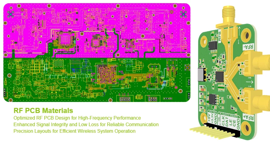
RF PCB design presents unique challenges that don't exist in digital or low-frequency analog circuits. At HILPCB, we manufacture RF boards for frequencies from 900MHz ISM band to 77GHz automotive radar. This guide shares practical solutions to the most common RF PCB design challenges based on thousands of wireless projects we've fabricated and assembled.
Whether you're designing WiFi modules, cellular amplifiers, or radar systems, understanding these challenges upfront prevents costly redesigns and schedule delays.
Challenge 1: Achieving Consistent 50Ω Impedance Control
Impedance control is fundamental to RF design, yet it's one of the most common sources of performance problems in manufactured boards.
Why 50Ω Matters:
- Maximum power transfer from source to load
- Minimum signal reflections (VSWR < 1.5:1 target)
- Predictable phase delay for phased array systems
- Industry standard for test equipment and connectors
Common Impedance Control Problems:
- Tolerance Stackup Errors
Impedance depends on multiple manufacturing variables:
- Trace width: ±0.025mm typical fabrication tolerance
- Dielectric thickness: ±10% standard, ±5% achievable with premium multilayer PCB process
- Copper thickness: ±3µm for 1oz copper (35µm nominal)
- Dielectric constant: ±0.05 typical batch variation
Combined effect: 50Ω ±5-7Ω typical, 50Ω ±3Ω with tight controls.
Solution: Design with realistic tolerances. Specify ±7% impedance tolerance (46.5-53.5Ω) unless your application absolutely requires tighter. Use our Gerber viewer to verify trace widths before fabrication.
- Wrong Material Selection
FR4 PCB dielectric constant varies with frequency:
- 1GHz: Dk = 4.4
- 5GHz: Dk = 4.2
- 10GHz: Dk = 4.0
- Loss tangent increases dramatically above 5GHz
Solution: Use controlled-Dk materials for >2GHz applications. RO4003C (Dk=3.38 ±0.05) provides consistent performance from DC to 40GHz. Consider high-frequency PCB materials for best results.
- Copper Surface Roughness Effects
Standard copper foil has 5-8µm RMS roughness. At high frequencies, this increases effective dielectric constant and loss.
Measured impact on 50Ω microstrip @ 10GHz:
- Smooth copper (1µm): 50.0Ω, -0.15dB/inch loss
- Standard copper (6µm): 52.5Ω, -0.28dB/inch loss
Solution: Specify low-profile copper for >10GHz designs. HVLP (Hyper Very Low Profile) copper reduces roughness to 2-3µm RMS.
Practical Impedance Design Tips:
- Use wider traces when possible (more tolerant to variations)
- Include test coupons on production panels
- Request TDR measurement reports with every order
- Design PCB with HDI technology for critical impedance sections
Our SMT assembly process includes pre-production impedance verification to catch problems before full production runs.
Minimizing Insertion Loss in RF Signal Paths
Insertion loss plays a crucial role in determining the performance of RF systems. Every dB of insertion loss reduces the range, sensitivity, and output power of your system. Understanding the causes of insertion loss helps optimize your RF PCB designs for minimal signal degradation.
Key elements of our strategy to minimize insertion loss include:
- Material selection to reduce dielectric loss and improve signal integrity at higher frequencies
- Trace width and copper weight optimization to minimize conductor losses
- Via transition design to ensure minimal signal path interruptions
By focusing on these key factors, we help ensure that RF PCBs maintain high performance with minimal signal degradation, improving system reliability and efficiency.
1. Material Selection for Dielectric Loss
Dielectric loss impacts signal strength, especially at higher frequencies. Choosing the right material can dramatically reduce insertion loss.
- Solution: For frequencies under 2GHz, standard FR4 materials are sufficient. For 2-20GHz, RO4003C is optimal, while for frequencies above 20GHz, RO5880 or other low-loss substrates are ideal for reducing loss.
2. Minimizing Conductor Loss (I²R Losses)
Conductor losses increase as trace resistance rises, particularly in high-frequency designs. At frequencies above 10GHz, current flows mainly on the surface of the conductor (skin effect), leading to additional losses.
- Solution: Use adequate copper weight: 1oz (35µm) for RF traces, and 2oz (70µm) for power amplifier feeds. For high-power applications (above 10W), consider heavy copper PCBs to reduce resistance and improve performance.
3. Optimizing Via Transitions
Each via in an RF signal path adds loss. Poorly designed vias can cause significant signal degradation, especially in high-frequency applications.
- Solution:
- Minimize the number of layer transitions to reduce signal loss.
- Use blind vias to eliminate stubs, particularly critical above 10GHz.
- Implement via back-drilling to shorten the signal path.
- Add ground via fencing around signal vias (6-8 ground vias with 0.5mm spacing).
- Consider using rigid-flex PCBs to minimize the need for vias and improve signal integrity.
Challenge 3: EMI and Crosstalk in Multi-Channel RF Systems
Electromagnetic interference between RF channels degrades system performance and causes regulatory compliance failures.
Common EMI/Crosstalk Sources:
- Inadequate Ground Plane Coverage
Missing ground creates return current loops and radiation:
- Solid ground plane: <-50dB isolation
- Split ground plane: -20dB isolation (unacceptable)
Solution: Never split ground plane under RF traces. Use solid ground on layer adjacent to RF signals. For multilayer PCB with mixed RF/digital, compartmentalize sections with via fencing.
- Insufficient Trace Spacing
Coupling between parallel traces:
| Spacing | Typical Isolation |
|---|---|
| 1× trace width | -15dB (poor) |
| 2× trace width | -25dB (marginal) |
| 3× trace width | -35dB (good) |
| 5× trace width | -45dB (excellent) |
Solution: Use 3-5× trace width spacing for critical RF paths. Route RF traces on opposite sides of PCB with ground between. Avoid long parallel runs.
- Ground Via Spacing
Via fence spacing affects shielding effectiveness:
- Via spacing > λ/4: Ineffective shielding
- Via spacing = λ/8: Good shielding (-40dB)
- Via spacing = λ/10: Excellent shielding (-50dB)
At 10GHz, λ = 30mm:
- Poor: Via spacing >7.5mm
- Good: Via spacing ~3.75mm
- Excellent: Via spacing ~3mm
Solution: Create via fences around RF sections. Use PCB viewer to verify via placement meets λ/8 or λ/10 spacing.
- Digital Noise Coupling
High-speed digital clocks contaminate RF circuits:
- Crystal oscillator harmonics land on RF frequencies
- Switching power supply noise couples through shared ground
- SPI/I2C data lines running near RF traces
Solution: Physical separation between RF and digital sections. Use halogen-free PCB materials for better signal integrity. Filter all power supplies entering RF sections.
EMI Design Checklist:
- Solid ground plane on layer adjacent to RF (no splits)
- Via fencing around RF sections (λ/8 or better spacing)
- 3-5× trace width spacing between RF channels
- Separate power domains for RF and digital
- Shield cans for sensitive RF circuits (if needed)
- Ferrite beads on power lines entering RF sections
Our turnkey assembly service includes EMC testing consultation and shield can installation.
Challenge 4: Thermal Management in High-Power RF Amplifiers
Power amplifiers generate significant heat that must be removed to prevent performance degradation and component failure.
Heat Generation Calculation:
Example: WiFi 5GHz power amplifier
- Supply: 3.3V × 1.5A = 4.95W input
- RF output: 100mW (20dBm) = 0.1W
- Efficiency: ~10%
- Heat dissipation: 4.85W
Thermal Design Strategies:
- Copper Area for Heat Spreading
Rule of thumb: 1W dissipation requires ~1 square inch of 1oz copper to limit temperature rise to 10°C in still air.
For 5W amplifier:
- 1oz copper: Need 5 sq.in. (not practical)
- 2oz copper: Need 2.5 sq.in. (better)
- Thermal vias to metal core PCB: 0.5 sq.in. (best)
Solution: Use heavy copper PCB (2-4oz) for power planes. Add thermal via arrays under power devices.
- Thermal Via Design
Single large via vs via array:
- One 0.6mm via: 70°C/W thermal resistance
- Four 0.3mm vias: 35°C/W (2× better)
- Sixteen 0.3mm vias: 10°C/W (7× better)
Solution: Dense thermal via arrays work best. For QFN packages: 0.3mm vias on 0.8mm pitch covering 70% of thermal pad.
- Material Selection
Thermal conductivity comparison:
- FR4: 0.3 W/m·K (poor)
- High-Tg FR4: 1.0 W/m·K (better)
- Rogers RO4003C: 0.64 W/m·K (moderate)
- Aluminum core: 200 W/m·K (excellent)
Solution: For >5W dissipation, use high thermal conductivity PCB materials or metal core construction.
- External Heatsink Interface
Thermal interface resistance:
- Direct PCB-to-heatsink: 5-10°C/W
- With thermal pad: 2-5°C/W
- With thermal grease: 1-2°C/W
Solution: Design PCB with adequate mounting for heatsink. Use thermal vias to transfer heat to bottom layer where heatsink attaches.
Thermal Via Array Example:
For 5W power amplifier in 5×5mm QFN package:
- Via size: 0.3mm diameter
- Via pitch: 0.8mm
- Array: 5×5 = 25 vias
- Fill: Copper-filled or thermal epoxy
- Expected thermal resistance: 8-10°C/W
This design keeps junction temperature <100°C with reasonable heatsink.
Challenge 5: Antenna Integration and Tuning
PCB antennas offer cost and space advantages but require careful design and tuning.
Common Antenna PCB Design Challenges:
- Ground Plane Size Effects
Antenna performance depends heavily on ground plane:
- Infinite ground plane: Ideal performance
- Finite ground plane: Detuning, pattern distortion
- Small ground plane: Severe detuning, poor efficiency
Example: 2.4GHz PCB antenna
- λ/2 = 62mm
- Recommended ground: 2λ × 2λ = 250mm × 250mm
- Actual PCB: 50mm × 80mm (severe detuning expected)
Solution: Simulate antenna with actual PCB dimensions. Use antenna tuning components (π-match network). Consider flexible PCB extensions for ground plane expansion.
- Nearby Metal Objects
Metal enclosures, battery, LCD screens all detune antennas:
- Resonant frequency shift: -50 to +100MHz typical
- Impedance change: 50Ω design becomes 30Ω or 75Ω
- Pattern distortion and efficiency reduction
Solution: Always simulate antenna in final enclosure. Add matching network with adjustable components for tuning. Use BOM viewer to track antenna tuning components.
- Manufacturing Tolerances
PCB antenna performance sensitive to:
- Trace width: ±0.025mm affects resonance by 5-10MHz
- Dielectric constant: ±0.1 changes impedance by 5Ω
- Substrate thickness: ±0.1mm shifts frequency
Solution: Use materials with tight Dk tolerance. Specify controlled dielectric thickness (±5%). Design antenna with tuning range to compensate for variations.
- Certification Testing Failures
Common failure modes:
- Radiated spurious emissions (harmonics too high)
- Poor TRP/TIS performance (antenna efficiency low)
- Excessive SAR (specific absorption rate) for body-worn devices
Solution: RF chamber testing during prototype phase. Our small batch assembly enables quick iteration for antenna optimization.
Antenna Design Best Practices:
- Keep antennas away from RF shields and metal parts
- Use ground-independent antenna types when possible (dipole, IFA)
- Include π-match or L-match tuning network
- Plan for tuning during production (DNP components)
- Test radiated performance in actual enclosure
Challenge 6: RF Connector Transitions and Pad Design
Poor connector footprints cause impedance discontinuities and signal reflections.
Critical Connector Design Elements:
- Pad Geometry
Standard PCB pads often wrong for RF:
- Center pin pad too large: Capacitance too high
- Ground pad spacing wrong: Impedance mismatch
- Via placement improper: Return path discontinuity
Solution: Use connector manufacturer's recommended footprint. Verify with EM simulation or 3D viewer. Add tuning stub if needed.
- Ground Via Placement
RF connectors need proper ground vias:
- Quantity: 4-6 vias minimum around center pin
- Spacing: <λ/10 at highest frequency
- Diameter: 0.3-0.4mm typical
- Distance from center: Matches connector geometry
Poor ground vias add 0.5-1.0dB insertion loss and degrade return loss to -8dB (unacceptable).
Solution: Follow connector datasheet via requirements exactly. Use HDI PCB processes for optimal via placement.
- Coplanar Waveguide Transitions
Edge-launch connectors require GCPW (grounded coplanar waveguide):
- Center trace
- Ground planes on both sides (not just bottom)
- Via fencing along trace
Without proper GCPW: -10dB return loss typical With optimized GCPW: -20dB return loss achievable
Solution: Use GCPW for all edge-launch RF connectors. Maintain 50Ω impedance through transition. Our high-frequency PCB team provides transition design support.
RF Connector Design Checklist:
- Use manufacturer recommended footprint
- 4-6 ground vias around center pin
- GCPW for edge-launch connectors
- Via fencing (λ/10 spacing) along transmission line
- Impedance verification through connector transition
- Mechanical stability (connector stress relief)
RF PCB Material Selection Quick Guide
Choosing the right material for your frequency range:
900MHz - 2.4GHz (ISM Bands):
- FR4 PCB with controlled Dk: Acceptable for most applications
- RO4003C: Better performance, recommended for sensitive receivers
2.4GHz - 6GHz (WiFi, Bluetooth, Zigbee):
- Standard FR4: Marginal (high loss above 5GHz)
- High-Tg FR4: Better thermal stability
- RO4003C or RO4350B: Recommended for best performance
6GHz - 20GHz (C/X/Ku bands):
- RO4003C: Standard choice, good performance/cost
- RO4350B: Lead-free compatible, automotive applications
- Consider Rogers PCB materials
20GHz - 40GHz (Ka band, 5G mmWave):
- RO4003C: Acceptable for lower end of range
- RO3003 or RO5880: Better for higher frequencies
Above 40GHz (V-band, W-band, automotive radar):
- RO5880: Standard for 77GHz radar
- PTFE-based materials required
- Low-profile copper essential
Material selection dramatically affects performance and cost. Our engineering team provides free material recommendations based on your specifications.
Why HILPCB for RF PCB Manufacturing
Specialized RF Capabilities:
- Rogers authorized fabricator (RO4000, RO3000, RO5000 series)
- Impedance control: ±3-7% depending on requirements
- High-frequency PCB up to 77GHz
- HDI technology: 0.1mm vias, fine-line capability
Quality Assurance:
- 100% TDR impedance testing on production boards
- RF chamber testing available (TRP, TIS, S-parameters)
- Material certificates and traceability
- IPC Class 2/3 manufacturing
Engineering Support:
- Free DFM review for RF designs
- Impedance calculation service
- Stackup optimization for cost reduction
- Antenna tuning and matching network design
Assembly Services:
- SMT assembly with RF-specific handling
- Through-hole assembly for connectors and shield cans
- Turnkey assembly with functional testing
- RF shielding and heatsink installation
From prototype to large volume assembly, we deliver RF PCBs that meet your performance requirements on time and on budget.
Frequently Asked Questions – RF PCB Design
Q1: What's the minimum trace width for 50Ω impedance?
A: Depends on substrate thickness and material. For RO4003C with 0.254mm substrate: 50Ω microstrip = 0.46mm trace width. For stripline: 0.18mm typical. Use impedance calculator or request calculation from us.
Q2: How many ground vias do I need around RF traces?
A: Via spacing should be <λ/10 at your highest frequency. For 10GHz (λ=30mm), space vias every 3mm or less. Minimum 4-6 vias around RF connectors for proper grounding.
Q3: Can I use FR4 for 5GHz WiFi applications?
A: Yes, but with limitations. Use high-quality FR4 with controlled Dk and low loss tangent. Performance better with RO4003C but FR4 acceptable for short traces and moderate power. Above 6GHz, Rogers materials strongly recommended.
Q4: How do I reduce EMI between RF and digital sections?
A: Physical separation (different board areas), solid ground plane (no splits), via fencing between sections, separate power domains with filtering, and shield cans over sensitive RF circuits if needed.
Q5: What surface finish works best for RF PCBs?
A: ENIG (Electroless Nickel Immersion Gold) recommended for RF applications—provides flat surface, good solderability, and low contact resistance for RF connectors. Avoid HASL (rough surface degrades high-frequency performance).