
Halogen-Free PCB Manufacturing | IEC 61249-2-21 | High-Tg, Low Smoke, RoHS/REACH
Halogen-free multilayer PCB manufacturing compliant with IEC 61249-2-21: chlorine/bromine below 900 ppm, high-Tg 170–200°C, low smoke/toxicity for automotive, medical and data-center systems. 3-day express service available.
Capabilities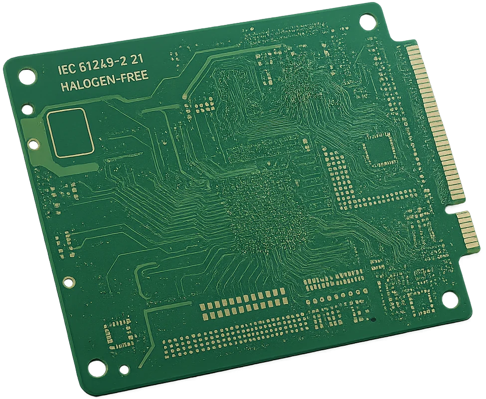
Why Halogen-Free: Compliance, Safety and High-Speed Performance
Lower smoke/toxicity with data-center and transportation readinessHalogen-free laminates reduce corrosive and toxic by-products in fire scenarios while meeting global environmental directives. All materials are qualified to RoHS compliance and REACH, with chlorine and bromine content strictly below 900 ppm as defined in IEC 61249-2-21.
Modern halogen-free systems deliver high-Tg 170–200 °C and Df 0.009–0.012 at 1 GHz, enabling 10–25 Gbps signal links with impedance control accuracy of ±5 %. For selection trade-offs versus standard FR-4, see our High-Tg PCB guide and FR-4 PCB comparison.
Critical Risk: Some halogen-free epoxy systems exhibit lower resin-to-glass adhesion and higher moisture absorption, which can cause CAF (Conductive Anodic Filament) growth or delamination during multiple reflow cycles and thermal shock.
Our Solution: We employ modified epoxy and phosphorus-nitrogen flame retardant systems with optimized resin flow and bonding strength. All halogen-free materials undergo IPC-4101 Class B/L qualification and interlaminar adhesion testing. Pre-bake and vacuum lamination remove absorbed moisture, while symmetric stackups minimize z-axis stress. These practices ensure equivalent or better reliability than conventional FR-4 in high-frequency PCB and automotive applications.
- Halogen content below 900 ppm
- High-Tg options: 170–200°C
- Df 0.009–0.012; Dk ≈4.1–4.4
- Low smoke/low toxicity for transportation and public venues
- Optimized for 10–25 Gbps channels
- Processes aligned with ISO 14001 environmental management
🚀 Quick Quote Request
📋 Get Full Capabilities
Process Control for Halogen-Free Reliability
Adhesion, copper integrity and clean-process chemistryLaser Direct Imaging achieves ±12.5 μm registration through sequential lamination. Controlled drilling and desmear maintain hole quality; adhesion after solder float targets >1.2 N/mm. Pulse-reverse plating keeps via copper thickness within ±10% for fatigue resistance and impedance stability.
Process chemistry is tuned for halogen-free resins to minimize ionic contamination and CAF risk. We provide 100% electrical testing, AOI/X-ray, and TDR coupon verification. For schedule/cost impacts, see our PCB assembly quote guide.
- LDI registration ±12.5 μm
- Via copper variation within ±10%
- Adhesion after solder float >1.2 N/mm
- CAF mitigation with low-ionic processes and resin systems
- 100% E-test, AOI, X-ray and TDR impedance checks
Halogen-Free PCB Capability & Performance Matrix
Manufacturing parameters from prototype to volume for low-toxicity, high-reliability applications
| Parameter | Standard Capability | Advanced Capability | Standard |
|---|---|---|---|
Layer Count | 2–12 layers | Up to 32 layers | IPC-2221 |
Base Materials | Halogen-free FR-4 Dk ≈4.2 | High-Tg 170–200°C, low-loss grades | IEC 61249-2-21 |
Board Thickness | 0.8–2.4 mm | 0.4–6.0 mm | IPC-A-600 |
Copper Weight | 1–2 oz (35–70 μm) | 0.5–6 oz (17.5–210 μm) | IPC-4562 |
Min Trace/Space | 100/100 μm (4/4 mil) | 50/50 μm (2/2 mil) | IPC-2221 |
Min Hole Size | 0.20 mm (8 mil) | 0.10 mm (4 mil) mechanical; 0.075 mm (3 mil) laser | IPC-2222 |
Impedance Control | ±10% | ±5% with TDR coupons | IPC-2141 |
Flammability & Smoke | UL 94 V-0; Low smoke density per ASTM E662 | Toxicity index per NES 713 (upon request) | UL 94 / ASTM E662 |
Halogen Content | Cl + Br <900 ppm | Process control to <700 ppm, lot-level reporting | IEC 61249-2-21 |
Quality Testing | 100% E-test, AOI | ICT, X-ray, TDR, SIR/CAF testing | IPC-9252 / IPC-TM-650 |
Certifications | ISO 9001, UL, RoHS/REACH | ISO 14001, IATF 16949, ISO 13485, AS9100 | Industry standards |
Lead Time | 3–7 days | 2–3 days express (project-dependent) | Production schedule |
Ready to start your PCB project?
Whether you need simple prototypes or complex production runs, our advanced manufacturing capabilities ensure excellent quality and reliability. Get your quote within 30 minutes.
Design Guidelines for Halogen-Free Materials
Halogen-free resins may show slightly different flow and Tg windows versus standard FR-4. Maintain impedance targets at ±5% with field-solver stackups and copper geometry control. For high-speed pairs, expect insertion loss near 0.1–0.2 dB/in at 10 GHz, layout-dependent. See our impedance control notes.
To minimize CAF, keep resin-rich areas balanced and avoid over-aggressive drilling. Where flame/smoke limits apply (rail/aviation), choose laminates with validated UL 94 V-0 and low smoke density; align with system standards documented in IPC standards mastery.
Need Expert Design Review?
Our engineering team provides free DFM analysis and optimization recommendations
Environmental and Reliability Qualification
Chemical screening verifies halogen limits <900 ppm and ionic cleanliness <10 μS/mm. SIR evaluates insulation resistance under 85°C/85% RH. Peel strength targets hold post-reflow, with microsections reviewing plating thickness and voids.
For safety-critical designs, we add ESS and temperature cycling (−40°C to +125°C), plus CAF testing per IPC-TM-650 2.6.25. Learn more in IPC-6012 acceptance guidance.
Industry Applications and System Considerations
Data center/telecom: low smoke density and 56 Gbps PAM4 channels with high-speed PCB design rules.
Transportation: reduced toxic emissions support enclosed-space safety; see our ISO 9001 manufacturing practices.
Medical: documentation under ISO 13485 with traceability to batches and test data.
Design to your system constraints—airflow, derating, and cabling—and use our assembly quote guide for cost/lead-time levers.
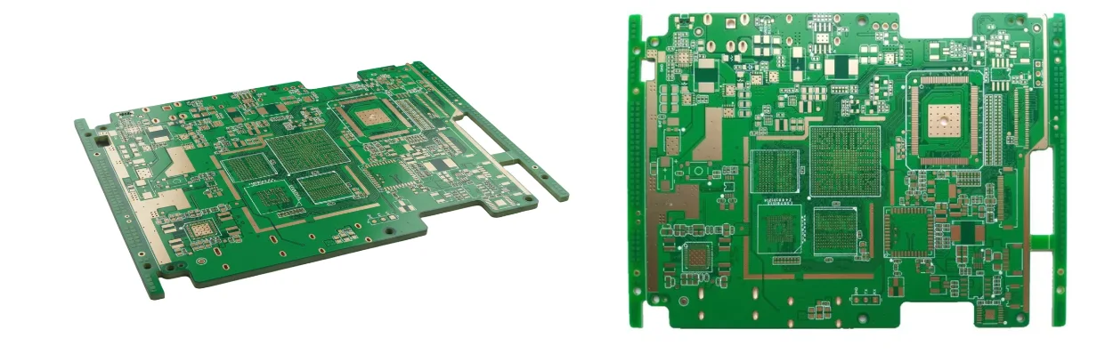
Engineering Assurance & Certifications
Experience: production-proven halogen-free stackups for multilayer and HDI with sequential lamination.
Expertise: TDR/VNA confirm impedance/loss; SPC governs plating and drill registration; Cpk targets ≥1.33.
Authoritativeness: builds align with IEC 61249-2-21, IPC Class 3, ISO 14001, IATF 16949 and ISO 13485.
Trustworthiness: MES links supplier lots and serialization to in-line test data; we provide lot-level halogen reports.
- Process controls: plating thickness, lamination temperature/pressure, LDI registration
- Traceability: unit serialization, component lot tracking, digital traveler
- Validation: ionic cleanliness, SIR/CAF, thermal cycling and ESS
Frequently Asked Questions
What defines a halogen-free PCB per IEC 61249-2-21?
Will halogen-free affect impedance or high-speed loss?
What documents do I need for a quote?
How do you address smoke density and toxicity?
Do you support HDI on halogen-free materials?
Experience Advanced PCB Manufacturing Excellence
From simple prototypes to complex production runs, our world-class factory delivers superior quality, fast turnaround and competitive pricing. Join thousands of satisfied customers who trust us with their PCB manufacturing needs.