

Rogers ro4350B is a hydrocarbon/ceramic laminate in the ro4000 family, engineered for RF, microwave and high-speed digital circuits that cannot meet their loss and tolerance budgets on standard FR-4. From a board designer’s point of view, an ro4350B PCB is interesting because it behaves much closer to an engineered RF substrate while still following a process flow that is compatible with conventional PCB manufacturing.
HILPCB is a PCB manufacturing and assembly factory with experience in RO4350B, RO4003C and related laminates, as well as FR-4, PTFE and ceramic substrates. This article focuses on technical aspects: how RO4350B behaves electromagnetically, how to structure stackups and transmission lines on it, how to mix it with other materials, and which process constraints should be taken into account when you prepare data for fabrication.
1. Electromagnetic behaviour of RO4350B PCB
RO4350B is designed to give stable, low-loss behaviour over a broad frequency range while remaining processable like a conventional glass-reinforced laminate. Key points for RF and high-speed engineers are:
- Dielectric constant window – RO4350B has a dielectric constant in the mid-3 range in the z-direction, with tight tolerance. Across the typical RF and microwave bands, Dk changes slowly with frequency, which simplifies controlled-impedance design and filter synthesis.
- Low dissipation factor – the loss tangent is on the order of a few 10⁻³ at multi-GHz frequencies, significantly lower than general-purpose FR-4. For microstrip and grounded coplanar waveguide (GCPW) lines, this directly reduces dielectric loss and improves link budgets in long RF paths.
- Low temperature coefficient of dielectric constant (TCDk) – the change in Dk between cold and hot conditions is small, so phase length and filter centre frequency do not drift excessively over operating temperature.
For time-domain and high-speed digital work, this translates to:
- predictable propagation delay and skew for differential pairs
- stable impedance over temperature, which reduces eye-diagram compression
- reduced need to “over-margin” equalisation settings to cover uncontrolled material variation
When HILPCB models an RO4350B PCB, we treat the material as a controlled RF dielectric rather than as a generic “FR-4 substitute”, and we encourage designers to base their EM models on thickness-specific Dk values rather than a single number for all thicknesses.
2. Stackup and transmission line design on RO4350B PCB
The stackup is part of the circuit for any RO4350B PCB carrying RF or high-speed signals. The goal is to obtain well-defined impedance and acceptable loss while keeping the structure manufacturable.
Common structures on RO4350B
On RO4350B we routinely fabricate:
- surface microstrip lines for RF power amplifiers, matching networks and antenna feeds (see also our notes on millimeter-wave RO4350B builds)
- embedded stripline channels for shielded RF or high-speed serial links inside multilayer PCB stacks
- GCPW traces for compact, well-confined routing and easier transitions to coax connectors
- tightly controlled differential pairs for high-speed digital interfaces that share the same board with RF sections
For each structure, the effective impedance depends on:
- core/prepreg thickness between trace and reference planes
- local Dk (including the effect of any solder mask above the trace)
- finished copper thickness including plating
- conductor shape and copper roughness at RF frequencies
Practical design notes
When you target standard impedance values (e.g. 50 Ω single-ended, 90–100 Ω differential), it is helpful to:
- specify the intended line type (microstrip, stripline, GCPW) and target impedance in the fabrication notes
- avoid extreme geometries; very narrow lines on thick cores or extremely tight gaps in GCPW can move the design into low-yield regimes
- decide early whether RF lines should be solder-mask defined, covered or left exposed; this affects the effective dielectric seen by the line
HILPCB can assist by reviewing your proposed stackup and line widths and mapping them to realistic manufacturing allowances under our high-frequency PCB capability. When required, we can also place impedance coupons so that TDR measurements confirm the realised impedance window.
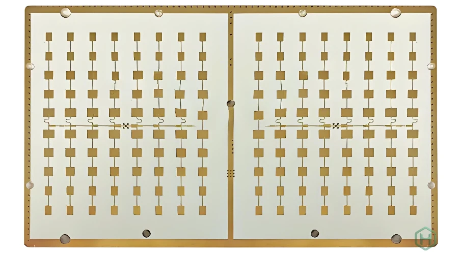
3. Mixed-material architectures: RO4350B with FR-4, RO3000 and PTFE laminates
Most systems do not use RO4350B on every layer. Instead, it appears as part of a mixed material architecture:
RO4350B + FR-4 hybrids
RO4350B is used on RF and selected high-speed layers, while FR-4 carries low-speed logic, housekeeping and power distribution. This approach reduces cost while keeping RF behaviour stable. Press cycles are tuned so that the different coefficients of thermal expansion (CTE) do not create stress in plated through-holes.RO4350B with other Rogers laminates
Some blocks may need different Dk or lower loss than RO4350B can provide. In such cases we combine RO4350B with RO4003C or RO3000 series materials on separate modules or, in some stackups, on selected layers. Our rogers circuit board service covers the RO4000, RO3000 and RT/duroid families, so we can keep material combinations consistent across a product family.RO4350B and PTFE/Teflon substrates
For very low-loss or very high-frequency structures (for example, narrowband filters or mmWave transitions), PTFE-based laminates are sometimes used in combination with RO4350B for the rest of the RF chain. These builds are handled via our teflon PCB processes, which account for the different via preparation and handling requirements of PTFE materials.
When designers provide a complete board-set view—RF modules on RO4350B, digital carrier on FR-4, optional PTFE sub-modules—we can keep connector impedances, mechanical stack heights and thermal paths aligned across the whole assembly.
4. Manufacturing and reliability constraints for RO4350B PCB
From a fabrication point of view, RO4350B is intended to follow a FR-4-like process, but there are details that matter for repeatable RF performance and long-term reliability.
Via and copper reliability
RO4000 laminates, including RO4350B, have a low z-axis CTE and in-plane CTE similar to copper, which supports robust plated through-holes even under severe solder-reflow and thermal-shock conditions.
For RF designs this matters because:
- via-in-pad structures under RF ICs and power devices are less likely to crack over life
- dense via fences and stitching around GCPW lines retain their electrical function over thermal cycling
- blind and buried vias in hybrid stacks can be designed without excessive risk of barrel fatigue, provided aspect ratios and drill sizes stay within controlled ranges
Conductor geometry and copper roughness
At GHz frequencies, conductor loss becomes comparable to dielectric loss. Design decisions that affect this include:
- choice between standard electrodeposited copper and smoother copper foils
- allowed etch tolerance on critical RF line widths
- whether heavy copper is really needed in RF sections or can be confined to power distribution layers
HILPCB characterises its processes so that etch compensation can be matched to the target impedance window. For very aggressive loss budgets, we can discuss copper options and surface preparation on a case-by-case basis.
Surface finish, assembly and system build
Surface finish affects both RF performance and assembly robustness:
- ENIG (electroless nickel immersion gold) is common for mixed RF/digital Rohs assemblies
- immersion silver can be useful for contact surfaces and some RF structures
- OSP is sometimes used where minimal additional interfaces are desired and the assembly flow is well controlled
Board-level assembly is then organised through our small-batch assembly lines for prototypes and early engineering builds, with migration to large-volume assembly when the design stabilises. For projects that need mechanical integration, cabling and enclosure work, we extend this into box-build assembly and full turnkey assembly, so the RO4350B PCB sits in a controlled chain from raw material to finished unit.
5. Design data, verification tools and collaboration with HILPCB
For a technical RO4350B PCB project, the most efficient way to interact with a manufacturer is to provide a well-defined design data set and to resolve RF-critical questions early.
Minimum recommended data
When you contact HILPCB for an RO4350B PCB, it is useful to include:
- fabrication data (Gerber, ODB++, or IPC-2581) for all copper and mask layers
- a proposed stackup showing which layers use RO4350B, FR-4 or other laminates
- impedance targets for each critical signal class (RF microstrip, stripline, GCPW, differential pairs)
- information about expected operating bands, maximum temperature, and whether the design must pass automotive or telecom-grade environmental stress
- assembly data (BOM, centroid/pick-and-place output, assembly notes) if you want PCBA in addition to bare boards
Before sending files, you can perform a quick visual check with our online Gerber viewer and 3D PCB viewer to ensure layer mapping, apertures and mechanical outlines look as intended; this reduces avoidable back-and-forth on basic data issues.
Technical discussion and support
If you need to:
- compare RO4350B with RO4003C, RO3000 or PTFE options for a specific block
- validate that a loss budget is realistic with the chosen line geometry and copper
- check whether a planned hybrid stackup is manufacturable with acceptable risk
our engineering team can review your material choices, stackup and routing strategy and provide feedback from a fabrication and assembly perspective.
If you have any questions about RO4350B PCB design, stackup definition, impedance control or manufacturability, you can contact HILPCB with your design goals and preliminary data. The earlier this technical exchange starts, the easier it is to align simulation assumptions with what can be built repeatedly on the production line.