
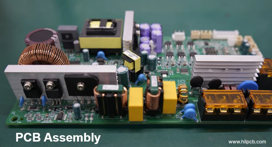
Driven by AI and HPC, advanced packaging is evolving at an unprecedented pace. From complex Chiplet architectures to high-bandwidth memory (HBM) integration, AI chip substrates and interconnect PCBs face massive design and manufacturing challenges. In this precision manufacturing ecosystem, Selective wave soldering has become a critical assembly technology. It not only solves mixed assembly between Through-Hole Technology (THT) parts and high-density SMT, but also provides process-level assurance for signal integrity, thermal risk control, and mechanical stability in high-reliability AI hardware production.
As AI compute demand grows exponentially, PCB designs become more complex and mixed-technology assembly becomes the norm. For example, high-power connectors and mechanical mounts for heat-spreading modules must coexist with precise SMT devices such as BGA and Chiplet components on the same HDI board. Traditional wave soldering exposes the entire PCB to high temperature—often fatal to thermally sensitive precision parts—while hand soldering cannot guarantee consistency and reliability at scale. Against this backdrop, Selective wave soldering emerged as the core process for modern AI chip interconnect and substrate PCB assembly challenges, thanks to its precise, controllable localized heating. As a company focused on high-difficulty PCB manufacturing and assembly, Highleap PCB Factory (HILPCB) has deep experience in this area and provides one-stop services from design optimization to final assembly.
What is the core role of selective wave soldering in HDI interconnect?
Selective wave soldering is an automated process that uses a small, precisely movable nozzle to apply molten solder to specific THT pin areas on a PCB without affecting surrounding SMT devices. Unlike conventional wave soldering that immerses the whole board, its core advantages are “selectivity” and “localization”.
The process typically includes three key steps:
- Fluxing: A micro-jet system applies flux precisely onto target pins and pads to ensure solderability and prevent oxidation.
- Preheating: Localized preheat activates flux and reduces thermal shock—especially important for thick copper boards or large ground planes on HDI PCB.
- Soldering: One or more mini nozzles move beneath each joint to form a small stable solder wave and complete the soldering precisely.
This point-to-point approach is ideal for THT parts on dense, double-sided SMT layouts. In AI substrates, it means high-power connectors can be soldered robustly without risking a nearby AI accelerator or HBM module that may cost thousands of dollars.
How does selective soldering protect Chiplet bridge PCB impedance control?
In Chiplet architectures, chiplets communicate over high-speed interconnect channels often implemented on a “bridge PCB” or an interposer substrate. Maintaining precise impedance on these channels is fundamental for SI. Any physical deformation or material property change during manufacturing can cause impedance mismatch, reflections, and data errors—making Chiplet bridge PCB impedance control a top priority.
Selective wave soldering acts as a “guardian” in this challenge. The large heat input from traditional soldering can warp the entire substrate (Warpage). Even small warpage changes transmission-line geometry (trace width, dielectric thickness), breaking carefully designed impedance matching. With localized heating concentrated into a few square millimeters, selective soldering dramatically reduces thermal shock to the whole substrate.
Concretely, the advantages include:
- Reduced substrate warpage: By minimizing the heat-affected zone (HAZ), overall flatness is preserved, keeping differential-pair symmetry and distance to the reference plane—key physical conditions for accurate Chiplet bridge PCB impedance control.
- Stable dielectric constant: High temperature can temporarily or permanently shift dielectric constant (Dk). Selective soldering avoids unnecessary heating of dielectric material under high-speed routes, maintaining electrical stability.
- Lower risk to adjacent BGA: In Chiplet packaging, tiny BGA joints are highly heat-sensitive. Selective soldering can safely solder nearby THT parts without reflowing the BGA array or inducing cold joints.
How soldering processes impact high-density PCBs: comparison
| Attribute | Selective Wave Soldering | Traditional wave soldering | Reflow soldering |
|---|---|---|---|
| Heat-affected zone (HAZ) | Very small; limited to the joint | Entire PCB bottom side | Entire PCB |
| Risk to SMT devices | Very low | High (masking required) | Medium (heat-sensitive parts) |
| Substrate warpage risk | Lowest | High | Medium |
| Applicability | Mixed-technology, high-density boards | Pure THT or single-side SMT | Pure SMT or secondary soldering |
| Process flexibility | Very high | Low | High |
Can this process protect automotive-grade HBM3 interposer PCB integrity?
Automotive electronics demands some of the strictest reliability standards of any industry. An automotive-grade HBM3 interposer PCB must carry extremely high bandwidth while operating long-term across wide temperatures (e.g., -40°C to 125°C), vibration, and high humidity. The HBM stack itself is connected to the interposer through thousands of micro-bumps, making it highly sensitive to thermal and mechanical stress.
Selective wave soldering has unique advantages for protecting these high-value, high-reliability assemblies:
- Minimized thermal stress: Any unnecessary thermal cycle creates thermo-mechanical stress between dissimilar materials (silicon, substrate, solder), potentially causing micro-cracks or delamination. Selective soldering confines heat to the THT connector area and avoids thermal damage to the HBM module and its precision interconnects.
- Process consistency: Automotive-grade products require extremely high repeatability. Automated selective-wave systems control parameters (preheat, solder time, wave height) to keep joint quality aligned with IPC-A-610 Class 3—well beyond typical hand-solder consistency.
- Compatibility with complex cooling hardware: AI chips often require vapor chambers (Vapor Chamber) or large heat sinks mounted through THT brackets. Selective soldering allows these mechanical fixtures to be soldered firmly without impacting already-assembled sensitive electronic components.
For an IATF 16949 certified manufacturer like HILPCB, adopting advanced processes such as selective wave soldering is a key step to ensure IC substrate PCB products meet harsh automotive standards.
What are the design rules for microvia HDI stack impedance control?
When designing a PCB for selective wave soldering—especially complex designs involving microvia and HDI stacking—you must follow specific DFM rules to ensure process feasibility and final reliability. Microvia HDI stack impedance control is not only an electrical design issue; it is a system engineering problem tightly linked to manufacturing processes.
Key considerations include:
- Keep-out zone: Define a clear safe area around target THT pins. No SMT devices, test points, or sensitive routing should be placed in this zone, to prevent nozzle collisions or thermal impact on adjacent parts. The required distance depends on nozzle size and tilt angle; 3–5 mm is commonly recommended.
- Thermal relief: For THT pads tied to large copper areas (ground or power), thermal relief pads are required. They prevent rapid heat sinking, allow solder to flow and form good joints, and help further limit heat spreading into the PCB.
- Placement optimization: Group all THT components requiring selective soldering into defined areas—ideally near board edges—to simplify paths, reduce nozzle travel distance/time, and improve production efficiency.
- Nozzle accessibility: Designers must ensure physical nozzle access. Tall nearby components can block the nozzle, so component height around THT parts should be controlled.
Accurate microvia HDI stack impedance control depends on end-to-end control from stack-up design through final assembly. Considering selective soldering requirements during design avoids expensive late-stage changes and helps ensure high yield and high reliability.
⚠️ Key selective-soldering design points
- ✅ Define a clear nozzle safety zone: Avoid physical interference with nearby SMT components.
- ✅ Use thermal relief pads: Form reliable joints on large copper areas while controlling heat spreading.
- ✅ Optimize THT placement: Group components to improve efficiency and process stability.
- ✅ Validate component height limits: Ensure the nozzle can reach all joints unobstructed.
Is selective soldering viable for industrial-grade RDL fan-out substrate integration?
Industrial-grade RDL fan-out substrate is an advanced packaging approach that enables smaller pitch and higher I/O density interconnects. While the RDL itself is built at wafer level (WLP) via semiconductor processes, the fan-out package must ultimately be assembled onto a system motherboard—typically a complex High Speed PCB carrying power, peripheral interfaces, and connectors.
In this scenario, selective wave soldering again shows its value. The system board may include high-mechanical-strength THT connectors (e.g., PCIe slots and power input terminals) located next to high-value fan-out modules. Selective soldering enables reliable soldering of those connectors without exposing the precision package to high-temperature risk.
For industrial-grade RDL fan-out substrate applications, advantages include:
- Protect precision packages: Avoid thermal damage to the fan-out package, its RDL layers, and micro-BGA joints.
- Enable higher density integration: Allows closer placement of THT connectors and advanced packages, improving PCB space utilization.
- Ensure long-term reliability: Provides robust I/O interfaces for industrial environments with frequent mating cycles or vibration.
How should HBM3 interposer PCB validation account for selective soldering?
HBM3 interposer PCB validation is a complex task spanning design, manufacturing, and test. It includes electrical validation (SI/PI) plus strict thermal and mechanical reliability testing. When selective wave soldering is part of the assembly flow, validation must consider its potential impact.
Key steps include:
- X-Ray inspection: After soldering, high-resolution X-Ray verifies internal quality of THT joints (fill, voids, cracks, bridges). It also checks nearby BGA joints to confirm they were not thermally deformed or damaged.
- Thermal cycling: The assembled PCB is cycled across high/low temperatures to simulate real operation. This exposes latent defects driven by CTE mismatch and is standard for evaluating automotive-grade HBM3 interposer PCB reliability.
- Cross-sectioning: Destructive microsectioning during validation provides direct metallographic evidence of joint quality, including IMC thickness and morphology.
- Signal integrity measurements: Using tools such as TDR, measure critical high-speed channels before and after soldering to confirm Chiplet bridge PCB impedance control remains within spec and that soldering did not degrade electrical performance.
A complete HBM3 interposer PCB validation plan must treat assembly processes as key variables that influence final product performance and reliability.
HILPCB capability matrix: enabling AI and HPC applications
| Parameter | Capability | Why it matters for AI substrates |
|---|---|---|
| Max layers | 56 layers | Supports complex power/signal partitioning to optimize SI/PI |
| Min trace/space | 2/2 mil (50/50 µm) | Enables high-density routing for HBM and Chiplet interconnects |
| Impedance control accuracy | ±5% | Protects high-speed signal quality; critical for microvia HDI stack impedance control |
| Laser drilling | Min via 50 µm | Supports HDI stacking and microvia designs—foundation for advanced substrates |
| Assembly services | SMT, THT, Selective Soldering | One-stop from PCB fabrication to complex assembly via [turnkey assembly service](/products/turnkey-assembly) |
Why choose a professional PCB manufacturer for complex assembly?
AI substrates and interconnect PCB manufacturing/assembly is highly specialized, combining materials science, electrochemistry, high-speed digital design, and precision manufacturing. From integrating industrial-grade RDL fan-out substrate to strict HBM3 interposer PCB validation, every step is challenging.
Choosing an experienced partner like HILPCB matters because:
- Integrated expertise: Professionals understand the linkage between design, fabrication, and assembly. They can provide DFM/DFA feedback early so designs can be built efficiently and reliably.
- Advanced equipment and processes: Selective-wave platforms, high-precision placement, and 3D X-Ray inspection are major investments. Professional manufacturers have the equipment plus mature process control to maintain high quality.
- Supply-chain management: Complex AI hardware requires special materials and components. HILPCB maintains a stable global supply chain, ensures availability of critical materials (e.g., low-loss laminates), and enforces strict incoming QC.
- One-stop services: Using the same supplier for PCB fabrication and assembly simplifies communication, shortens time-to-market, and clarifies quality responsibility—from bare board to final SMT assembly.
Conclusion: selective wave soldering is a key enabler for next-gen AI hardware
In short, Selective wave soldering has evolved from a niche add-on process into a core technology in modern high-performance electronics manufacturing. In AI, HPC, and automotive electronics, its precise localized heating solves the mixed-assembly challenge between dense SMT and THT parts. Whether stabilizing Chiplet bridge PCB impedance control or protecting automotive-grade HBM3 interposer PCB integrity, the value is significant.
As AI hardware moves toward higher integration, higher power, and more complex form factors, requirements for manufacturing and assembly precision and reliability will only get stricter. Selective wave soldering will remain a foundational enabling technology that helps turn advanced design blueprints into real products. Partnering with a manufacturer like HILPCB—backed by deep technical expertise and advanced capability—is key to succeeding in a competitive market.
Common Questions
Why does selective wave soldering matter in AI chip interconnect systems?
AI boards often mix advanced packages with through-hole connectors or power interfaces that still need strong mechanical joints. Selective wave soldering lets teams solder those connectors without exposing nearby high-value packages to unnecessary thermal stress.
Can assembly processes affect HBM3 interposer or chiplet-related validation?
Yes. Assembly is part of the final hardware system, so thermal load, solder geometry, and local stress can influence long-term reliability and even measured electrical behavior. That is why validation plans should include post-solder inspection and comparison.
What inspections are most useful after selective soldering on advanced AI boards?
X-ray, cross-section analysis, and high-speed electrical measurements are especially valuable. They help verify internal joint quality while also checking that nearby fine-pitch or high-speed structures were not degraded during assembly.
Why is one-stop manufacturing support helpful for AI interconnect projects?
These programs involve tightly coupled decisions across materials, fabrication, assembly, and test. A supplier that can see the whole chain can usually catch risks earlier and reduce iteration time during prototype and ramp-up.