
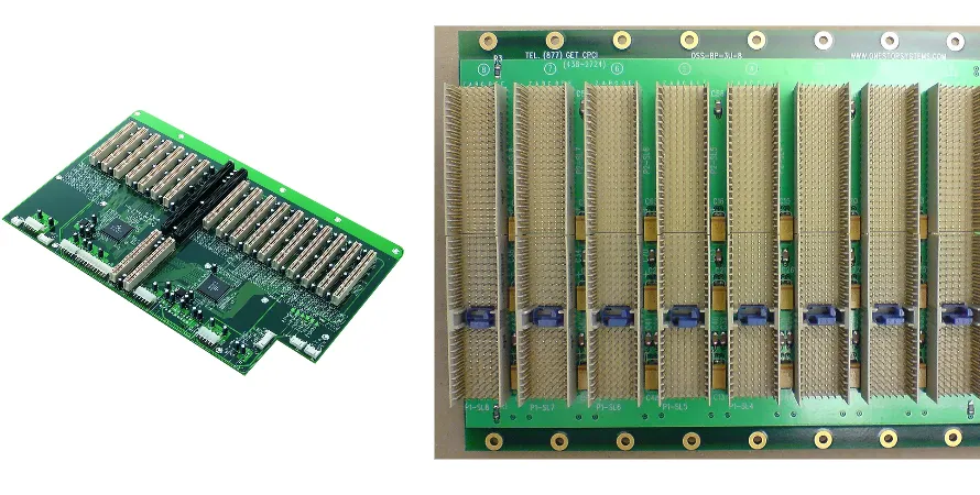
With explosive growth in AI and ML, data-center demand for compute has been rising exponentially. As the backbone of that compute, AI servers are pushing backplane PCB design and manufacturing into new territory. These backplanes must carry kilowatts of power while maintaining loss-minimized transmission for ultra-high-speed protocols such as PCIe 5.0/6.0 and future CXL (Compute Express Link). In such complex, high-density mixed-assembly environments, traditional soldering processes are increasingly stretched—and Selective wave soldering has emerged as a key enabler for backplane reliability and performance.
From the perspective of a high-speed materials and stack-up planning specialist, this article explains the core role of selective wave soldering in AI server backplane manufacturing. We’ll cover how it helps address tough challenges in signal integrity (SI), thermal management, and power integrity (PI), and we’ll outline end-to-end optimization strategies across design, routing, and fixture development. For teams aiming to succeed in AI server motherboard PCB mass production, mastering selective wave soldering is a must. Highleap PCB Factory (HILPCB) has accumulated extensive hands-on experience in this domain and can provide one-stop support from prototypes to volume production.
What is selective wave soldering and why it matters for AI servers?
Selective wave soldering is a highly automated Through-Hole Technology (THT) soldering process. Unlike conventional wave soldering that immerses the entire PCB into a solder wave, selective wave soldering uses one or more mini programmable nozzles to solder only pre-defined joints. It is typically performed after the PCB has completed SMT assembly, making it an ideal process for mixed-technology boards.
In AI server backplanes, its value is particularly clear:
- Protect dense SMT devices: AI server backplanes are packed with BGA, LGA, high-speed connectors, and many passives. The point/area-selective nature of selective wave soldering avoids these heat-sensitive devices, preventing unnecessary secondary reflow thermal shock and improving yield and long-term reliability.
- Handle complex, high-thermal-mass boards: AI server Backplane PCB designs often exceed 20 layers, use thick boards (>4 mm), and include large copper power planes. This high thermal mass is difficult to solder reliably. With concentrated energy and optimized preheat, selective wave soldering can heat through thick stacks and achieve full, Class-3 quality joints on THT connectors (power interfaces, high-speed card-edge connectors), meeting IPC-A-610 Class 3 barrel-fill requirements.
- Enable double-sided mixed assembly: Modern AI server architectures maximize space utilization by placing SMT and THT on both sides of the backplane. Selective wave soldering is the only practical, high-efficiency automated approach for such complex double-sided mixed assembly, and it increases flexibility in
AI server motherboard PCB routing.
Whether for rapid iteration in AI server motherboard PCB low volume prototypes or stability-driven mass production, selective wave soldering is an indispensable process.
How selective wave soldering affects high-speed signal integrity
For a high-speed AI server motherboard PCB carrying Tb/s-class throughput, even small impedance discontinuities can cause reflections, crosstalk, and ISI, ultimately destabilizing the system. The process control precision of selective wave soldering directly affects high-speed link SI.
Key impacts include:
- Minimize thermal stress to protect dielectric performance: High-speed PCBs often use low-Dk/Df materials such as Megtron 6/7. While electrically excellent, these materials can be sensitive to thermal stress. The localized heating of selective wave soldering reduces the range and duration of thermal cycling on the entire board, helping maintain stable dielectric properties and consistent differential impedance.
- Ensure electrical continuity of vias (Via): After signals enter the PCB through connector pins, they often traverse vias into inner-layer routing. Selective wave soldering provides sufficient concentrated heat to ensure complete barrel fill along the plated hole wall (Barrel Fill), creating uniform, void-free electrical connections. Incomplete fill behaves like a tiny “antenna” or “stub” at GHz frequencies, creating severe reflections.
- Control solder-joint geometry consistency: By tightly controlling nozzle flow, angle, and motion paths, the process produces highly consistent joints. Consistency reduces electrical path-length variation (skew) between channels—critical for timing on parallel interfaces such as DDR memory buses.
A well-optimized selective wave soldering process is a key “last mile” guarantee for high-speed signals from connectors to chips.
How soldering processes affect high-speed SI: comparison
| Parameter | Selective Wave Soldering | Traditional wave soldering | Hand soldering |
|---|---|---|---|
| Impedance consistency | High (parameterized process, stable joint geometry) | Medium (whole-board heating; non-uniformity from warpage) | Low (operator-dependent; poor consistency) |
| Barrel fill (Barrel Fill) | Excellent (strong localized heating; high fill rate) | Good (but challenging on high-thermal-mass boards) | Unstable (hard to control internal fill) |
| Impact on substrate Dk/Df | Minimal (localized heating; small HAZ) | High (entire board at high temperature; material drift risk) | Medium (local overheating risk) |
| Risk to nearby SMT devices | Very low (shielded by fixture + precise nozzle) | High (requires complex and unreliable masking) | Medium (heat radiation and handling risks) |
Thermal-management challenges in AI server backplanes and their link to soldering
AI server power density is pushing physical limits. A single GPU or ASIC can exceed 700W, and a full chassis can easily exceed 10kW. As a key path for power distribution and heat spreading, backplane design and manufacturing must prioritize thermal management.
Selective wave soldering plays a subtle but important role:
- Avoid thermal damage: When soldering high-current connectors, poor heat control can damage nearby VRM, inductors, or temperature sensors. Selective wave soldering delivers heat precisely so only target joints reach soldering temperature while adjacent areas stay within safe temperature rise.
- Preserve thermal-path integrity: Many THT components (e.g., high-power connectors) also contribute to heat transfer; their pins connect through solder joints to large copper heat-spreading layers on the PCB. Selective wave soldering forms void-free, thermally conductive joints so heat transfers efficiently into the Heavy Copper PCB layers, avoiding localized hot spots.
- Adapt to high-thermal-mass designs: To carry high current, power and ground layers often use 4 oz copper or thicker. This dramatically increases thermal mass, and conventional methods struggle to heat effectively. Selective wave equipment typically includes strong bottom/top preheat modules plus high-energy nozzles to deliver sufficient energy for reliable soldering on these “heat sponges”.
Optimizing PCB routing and layout for selective wave soldering
Design for Manufacturability (DFM) bridges design and manufacturing. Considering selective wave soldering requirements during AI server backplane design can greatly improve production efficiency and final quality. This requires deep optimization of AI server motherboard PCB routing and component placement.
Key design guidelines include:
- Define clear soldering regions: Create sufficient keep-out zones around each THT component to accommodate nozzle size and motion. Typically, keep at least 2–3 mm clearance from the edge of a THT pad to avoid interference with nearby SMT devices.
- Optimize thermal relief: When a THT pin connects to a large copper plane, use thermal relief (“spoke” pads) to limit heat sinking during soldering while maintaining electrical connectivity, improving wetting and joint formation.
- Component orientation and grouping: Arrange THT components requiring selective soldering in consistent orientations and grouped regions. This simplifies nozzle paths, reduces cycle time, and improves
AI server motherboard PCB mass productionefficiency. - Avoid shadowing effects: Taller components can block the solder wave from reaching shorter joints, creating “shadows”. Consider component height and place taller parts downstream of solder flow or provide larger spacing.
As an experienced manufacturer, HILPCB provides comprehensive DFM analysis to identify and resolve selective-soldering risks early, shortening time-to-market and reducing manufacturing cost.
Selective wave soldering DFM checklist
- ✓ Fixture tooling holes: Place at least 3 asymmetric, high-precision tooling holes along the PCB edge for accurate alignment of soldering and test fixtures.
- ✓ Component spacing: Keep >5 mm from THT pad edge to nearest SMD pad edge so fixture walls have adequate room.
- ✓ Pad design: THT pad diameter should be 0.4–0.8 mm larger than pin diameter to support capillary action and solder fill.
- ✓ Avoid vias in pads: Do not place vias directly in THT pads (Via-in-Pad); this can drain solder and create incomplete joints.
- ✓ Process edge: Provide sufficient process edges for conveyor transport and fixture clamping to prevent board bending.
Why dedicated fixture design is central to selective soldering
If the selective wave soldering machine is the “scalpel”, then the dedicated fixture/pallet is the “locator and shield”. A well-designed fixture is a prerequisite for high-quality, highly repeatable soldering—its importance cannot be overstated. This aligns with the philosophy behind Fixture design (ICT/FCT): precision and stability in both manufacturing and testing.
The fixture’s main functions include:
- Accurate location and support: Using tooling holes to clamp the PCB, fixtures prevent warpage or shifting under high temperature and solder-wave impact—especially critical for large, heavy AI server backplanes.
- Selective masking: Fixtures open windows only where target THT joints must be soldered. All other areas—especially SMT devices, gold fingers, and test points—are covered to protect against flux contamination and molten-solder attack.
- Guiding solder flow: In some cases, fixture geometry can guide solder-wave flow and improve heat exchange at hard-to-solder pins.
Fixtures are typically CNC-machined from high-temperature, anti-static, low-warp composite materials such as Durostone or Ricocel. Design must consider PCB layout, component heights, nozzle type, and motion paths. A successful Fixture design (ICT/FCT) should also consider downstream test compatibility to maximize end-to-end efficiency.
Process parameter control: the key to high-quality soldering
Selective wave soldering is a multi-variable process where small parameter changes can affect joint quality. Establishing a stable and reliable process window for an expensive high-speed AI server motherboard PCB is a key measure of a manufacturer’s capability.
Core parameters include:
- Flux application: Flux volume and coverage must be controlled precisely. Too little causes poor wetting and bridges; too much can contaminate the board and impact electrical performance and long-term reliability. Drop-jet systems offer higher precision than traditional spray.
- Preheat: Preheating is critical to (a) activate flux, (b) ramp board temperature to reduce thermal shock at the solder wave, and (c) reduce thermal gradients to help solder flow. Profiles must be customized based on thickness, copper area, and component density.
- Soldering: Solder temperature, wave height, contact time, and travel speed are the four key variables. Pins tied to large copper areas may require slightly higher temperature and longer contact time to achieve full barrel fill.
- Nitrogen protection: Soldering in N2 significantly reduces oxidation, produces brighter, more reliable joints, and widens the process window. For near-zero-defect AI server production, N2 is almost standard.
Fine control and optimization of these parameters is the foundation for consistent quality from AI server motherboard PCB low volume builds through mass production.
Key selective-wave process window
| Parameter | Typical range | Impact on solder quality |
|---|---|---|
| Preheat temperature (top) | 100 - 140 °C | Too low reduces flux activation; too high may damage components. |
| Solder temperature (SAC305) | 260 - 280 °C | Affects flow and wetting; too high increases oxidation. |
| Contact time | 2 - 5 s | Determines fill depth; too long can damage PCB or components. |
| Nitrogen concentration | < 500 ppm O2 | Reduces oxidation and dross; improves appearance and reliability. |
Quality assurance and inspection: from AOI to X-Ray
Strict quality control is the final—and most important—line of defense for reliable AI server backplanes. For selective-wave joints, a multi-layer inspection strategy is required.
- Automated Optical Inspection (AOI): High-resolution imaging and rule-based comparison quickly detect surface defects such as bridges, cold joints, solder balls, and excessive/insufficient solder.
- Automated X-Ray Inspection (AXI): Internal quality (e.g., barrel fill percentage) of THT joints cannot be assessed optically. AXI is the ultimate tool for hidden defects. X-ray imaging reveals fill, bubbles, and voids—critical to long-term reliability for signal transmission and power distribution on High Speed PCB.
- Functional test (FCT): After assembly, dedicated fixtures (another key application of
Fixture design (ICT/FCT)) validate full electrical performance under simulated operating conditions, confirming all soldered connections function correctly. - Microsection analysis: During process development and periodic audits, sampled joints are cross-sectioned for metallographic inspection. IMC layer thickness and morphology provide a scientific basis for evaluating long-term reliability.
How HILPCB addresses the challenges with one-stop services
Given the multi-dimensional challenges in AI server backplane design, manufacturing, and assembly, choosing a partner with full-stack technical capability is critical. HILPCB provides exactly that.
We understand that Selective wave soldering is not an isolated step—it is a system engineering problem tightly coupled with PCB design, material selection, fabrication, and test. Our strengths include:
- Front-end co-design: Early collaboration with customer design teams to provide DFM/DFA recommendations, especially around
AI server motherboard PCB routingand placement, ensuring the design is selective-soldering-friendly. - Materials and process expertise: Deep familiarity with high-speed/high-frequency materials, enabling optimal material selection for
high-speed AI server motherboard PCBand the matching fabrication and soldering process parameters. - Precision fixtures and equipment: Investment in leading selective-wave platforms plus an in-house
Fixture design (ICT/FCT)team to deliver high-precision soldering and test fixtures for stable, repeatable processes. - Flexible capacity: From fast
AI server motherboard PCB low volumeprototypes to large-scaleAI server motherboard PCB mass production, HILPCB provides reliable, scalable capacity. - Strict quality system: Integrated inspection coverage including AOI, 3D AXI, ICT, and FCT, aligned with IPC-A-610 Class 3, ensuring every delivered SMT assembly board meets demanding quality requirements.
Conclusion
In the AI compute race, AI server backplanes act as the “nervous system” for massive data flow, and manufacturing capability directly determines system performance and reliability. With unmatched precision, flexibility, and protection for sensitive devices, Selective wave soldering has become indispensable. It addresses the challenges of high density, high thermal mass, and mixed-technology assembly—and is key to protecting SI and stable power distribution.
But successful selective-wave implementation is not easy. It requires deep integration across PCB design, materials, fixture engineering, process control, and stringent inspection. Choosing a partner like HILPCB, with strong technical accumulation and one-stop capabilities, helps mitigate risk, accelerate innovation cycles, and ultimately build a competitive advantage.
Common Questions
Why is selective wave soldering useful on AI server backplanes?
AI server backplanes often combine heavy through-hole connectors with dense high-speed SMT circuitry. Selective wave soldering allows robust connector joints while reducing thermal exposure to surrounding high-value devices and laminates.
Why are process parameters so critical on these boards?
Backplanes have high thermal mass, strict reliability targets, and expensive assemblies, so even small shifts in flux, preheat, or contact time can change joint quality. Stable parameter control is essential for repeatable yield and long-term field performance.
What role do pallets and test fixtures play in AI server backplane assembly?
Pallets protect sensitive regions during soldering and expose only the intended joints, while test fixtures confirm that the assembled board still meets electrical requirements. Both need to be considered early because they affect manufacturability and downstream validation.
What inspections are most important after selective soldering on a backplane?
AOI, AXI, and functional test are especially important because many critical defects are not visible from the surface alone. For high-reliability server hardware, hidden hole-fill or void issues need to be caught before shipment.