

As televisions evolve into intelligent, connected platforms, the underlying Smart TV PCB must deliver high performance, integration, and reliability. A PCB TV board integrates the main SoC, memory, wireless modules, and power management on a multilayer substrate, while companion boards in the TV PCB board set carry the T-con and backlight driver circuits. Understanding the PCB in TV products helps engineers specify the right layer count, substrate material, and thermal management approach for different screen sizes and feature sets, and the choice of PCB technology directly affects display reliability and long-term performance. At HilPCB PCB Factory (HILPCB), we specialize in fabricating and assembling Smart TV circuit boards tailored for 4K/8K displays, streaming modules, and voice-enabled user interfaces.
We combine multilayer PCB technology, RF expertise, and rigorous quality control to support global Smart TV OEMs from prototyping to large-scale production.
Smart TV PCB Architecture and Design Principles
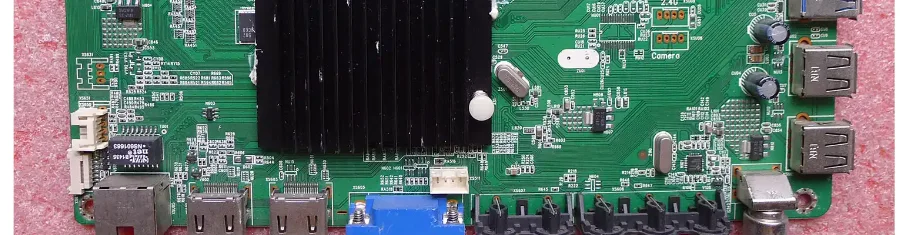
The Smart TV PCB acts as the central processing hub, coordinating video rendering, wireless communication, and system logic. Modern Smart TVs feature complex, compact boards integrating:
- High-performance SoCs with AI upscaling engines
- DDR4/LPDDR memory, NAND flash storage
- HDMI 2.1, USB 3.0, and Ethernet ports
- Dual-band Wi-Fi, Bluetooth, ZigBee modules
- Multi-rail power delivery networks
Most designs adopt multilayer PCB stackups (6–12 layers) with HDI routing and ground-signal-ground topologies for signal integrity.
Design Focus Areas:
- Controlled impedance for high-speed interfaces (e.g. HDMI)
- EMI shielding for RF zones and display drivers
- Heat spreading under SoC, RAM, and PMICs
- Isolation between analog AV paths and digital logic
Wireless and Connectivity
- Dual-band Wi-Fi 6 and BT 5.0 integration
- ZigBee/Thread for smart home hubs
- Optional 5G and NFC modules
Thermal and EMI Control
- High-Tg FR4 PCB materials for thermal resilience
- Copper pour zones and stitched thermal vias
- Segregated RF/digital shielding strategy
Smart TV PCB Fabrication and Material Considerations
Manufacturing Smart TV PCBs requires strict process control across mechanical, thermal, and electrical domains. These boards often span large surface areas and include both surface-mount and through-hole elements.
Fabrication Characteristics:
- 6 to 12-layer boards with low-loss high-frequency PCB materials
- ±10% impedance tolerance for HDMI, USB, and DDR signals
- ENIG/ENEPIG surface finishes for high-density BGA placement
- High-Tg PCB core materials for elevated reflow and ambient temperatures
Advanced builds may incorporate hybrid stackups or localized shielding enclosures. Our facility supports sequential lamination and via-in-pad structures to accommodate high net counts in constrained footprints.
Assembly highlight: precision meets scalability. Smart TV mainboards vary from compact embedded types to full-sized modular backplane assemblies. Our SMT lines accommodate fine-pitch SoCs, while box-build assembly services support integration into final chassis.
Key Assembly Capabilities:
- 0.3 mm BGA and 0201 passive placement accuracy
- Dual-sided reflow, selective wave soldering for legacy I/Os
- X-ray inspection for hidden joints and cavity packages
- Functional testing including HDMI loopback and RF verification
For enhanced durability, we also offer optional conformal coating and thermal interface application for heatsink-ready components.
Smart TV Applications and Deployment Environments
The Smart TV PCB must meet a wide spectrum of performance and environmental expectations, from consumer homes to hotel rooms and public signage.
Deployment Categories:
- Premium 4K/8K Smart TVs – High frame rate processing and voice assistant support
- Commercial Displays – Extended runtime and reliability for signage/video walls
- Hospitality & Embedded TVs – Custom firmware and remote control integration
- Gaming Displays – 120Hz+ refresh, VRR, G-Sync/FreeSync support
SMT Assembly and box-build assembly options support both OEM and ODM models, while modular architecture allows rapid configuration across SKUs.
Engineering Services and Manufacturing Support
HILPCB supports basic through premium Smart TV boards, including 8K, HDR and audio applications, with PCB fabrication and assembly planned around the specified interfaces and product configuration. Interface, thermal, humidity and vibration tests are available when included in the agreed validation plan. A −20 °C to +70 °C thermal-test option is illustrative and applies only to eligible product plans; it is not a default operating rating or a guarantee for every assembled product.
At HILPCB, we offer full-stack support for Smart TV PCB development, including early-stage simulation and post-assembly validation.
Comprehensive Services Include:
- Signal simulation using impedance calculator
- Visual validation via Gerber viewer
- Component planning with BOM viewer
- Functional and stress testing with production-grade diagnostics
All production complies with IPC-A-610 and RoHS standards, with traceable lot control and anti-counterfeit component sourcing.
Common Questions
What functions does a Smart TV PCB usually combine on one board?
A Smart TV board typically combines the main SoC, memory, storage, high-speed display interfaces, wireless modules, Ethernet, and multi-rail power delivery. That level of integration makes layout, EMI control, and thermal design critical.
How does a Smart TV PCB differ from a traditional television circuit board?
Smart TV boards integrate a full computing platform, wireless connectivity modules, and advanced video processing that traditional television boards never carried. That means ARM-based processors with dedicated graphics acceleration, substantial memory resources, and extra interfaces for streaming services, which raises the bar on power integrity and signal routing.
Why do Smart TV PCBs often use multilayer and HDI structures?
They need enough routing density and controlled impedance for HDMI, DDR, USB, RF, and other fast interfaces in a compact footprint. Multilayer stackups also help isolate noisy digital areas from analog or wireless sections.
What do the terms PCB TVs, TVs PCB, and TV PCB board mean in supplier listings?
They all refer to the same product class: the printed circuit boards inside a television. Buyers, engineers, and suppliers write the words in different orders on RFQs, part numbers, and marketplace listings, so PCB TVs or a TVs PCB assembly in a quotation describes the same smart TV circuit board a design team would call the main board.
What tests are important after Smart TV PCB assembly?
Manufacturers commonly perform AOI, X-ray inspection for hidden joints, interface validation, HDMI loopback, RF checks, and broader functional tests. Thermal and reliability checks are also important for long operating hours.
How do you manage thermal challenges in Smart TV PCB design?
Thermal management combines strategic component placement, thermal via implementation, and specialized substrate materials. High-power components like processors and LED drivers are positioned to maximize heat spreading while thermal vias conduct heat to chassis mounting points, and advanced builds may add dedicated heat sinks or thermal interface materials for critical components.
How should OEMs qualify a smart TV box Pro board PCB assembly manufacturer?
Ask for the SMT line's fine-pitch capability, in-circuit and functional test coverage, firmware loading and serialization support, and experience with HDMI, Wi-Fi, and DRM-related compliance testing. A qualified smart TV box Pro board PCB assembly manufacturer should also show traceable component sourcing and lot control, and define controls for counterfeit-component risk.
Can one manufacturing flow support both consumer TVs and commercial displays?
Yes, if the supplier can scale from compact mainboards to larger assemblies while controlling quality and traceability. The exact materials, burn-in depth, and test profile may differ by application segment.