
As 5G evolves toward 6G, operating frequencies are moving into the millimeter-wave (mmWave) and even sub-THz domains. This shift raises unprecedented challenges for PCB design and manufacturing. In this context, a strong, precise quality-control system is essential—and SPI/AOI/X-Ray inspection (solder paste inspection / automated optical inspection / X-ray inspection) is one of its core pillars. It is no longer a simple end-of-line check; it is a data-driven assurance mechanism spanning the entire lifecycle from design validation to mass production, ensuring every high-speed-signal PCB achieves low-loss, high-reliability interconnects under harsh conditions. For complex designs using hybrid lamination (Hybrid Stack-up) with RF materials such as Rogers/PTFE and standard FR-4, the coordinated use of these three inspection technologies is often the deciding factor between success and failure.
DFM/DFT/DFA review: ensuring mmWave PCB manufacturability from the start
In any advanced PCB manufacturing flow, prevention beats rework. A comprehensive DFM/DFT/DFA review (design for manufacturing / test / assembly review) is the foundation for successful mmWave PCB programs. The goal of this phase is to identify and eliminate any risks that could impact yield, performance, and reliability before design freeze. For 5G/6G applications, the focus goes far beyond traditional PCBs.
First, material selection is central. Low-Dk/Df materials such as Rogers and Teflon (PTFE) deliver excellent electrical performance, but their mechanical behavior differs greatly from standard FR-4. For example, PTFE is relatively soft; drilling can easily create smear, burrs, and rough hole walls—directly impacting plating quality. During DFM/DFT/DFA review, we must validate whether drilling parameters and hole preparation (e.g., plasma desmear) match the chosen material set.
Second, the review must examine stack-up details. In hybrid lamination, differences in coefficient of thermal expansion (CTE) can accumulate stress during lamination, leading to warp or even delamination. DFM review uses simulation to predict these risks and optimize the press cycle (Press Cycle) and resin flow (Resin Flow) model.
Finally, this review establishes the baseline for downstream SPI/AOI/X-Ray inspection. For example, the minimum pad size, solder mask opening tolerance, and BGA land design defined in DFM directly shape SPI parameters and AOI defect-recognition performance. A high-quality DFM/DFT/DFA review is the starting point of the entire new product introduction (NPI) flow. It lays a solid foundation for NPI EVT/DVT/PVT, ensuring design intent can be translated into a reliable physical product.
Hybrid Stack-up challenges and inspection strategy
To strike the best balance between performance and cost, 5G/6G communication products (e.g., AAU base-station antenna units) commonly adopt hybrid stack-ups. This approach typically uses high-performance RF materials (such as Rogers PCB) for outer layers carrying mmWave signals, while using lower-cost FR-4 for inner layers handling digital and power routing. However, this “mix-and-match” introduces unique manufacturing and inspection challenges.
Layer-to-layer registration accuracy: Different materials expand and shrink differently during lamination, causing registration offset. Even a small offset can degrade via-to-inner-pad connections, compromising impedance continuity along the signal path. X-Ray inspection is essential here: it can penetrate multilayer boards to measure inner-layer alignment precisely and feed back data to adjust process parameters in real time.
Via plating quality: Drilling through the PTFE/FR-4 interface demands extremely tight control. Small variations in tool wear, spindle speed, and feed rate can create resin smear on hole walls, preventing reliable copper adhesion. Beyond microsectioning, high-resolution X-Ray inspection can also support non-destructive evaluation of via uniformity and latent defects across production lots.
Press-window control: Hybrid lamination has a narrow process window. Precise control of temperature, pressure, and time is critical to ensure strong bonding between materials and avoid delamination or voids. With integrated Traceability/MES (traceability / manufacturing execution system), we can record each board’s press profile and correlate it with X-Ray findings—continuously optimizing the process.
Material properties comparison: RF materials vs. standard FR-4
| Parameter | Rogers/PTFE materials | Standard FR-4 materials |
|---|---|---|
| Dielectric constant (Dk) @10GHz | 2.2 - 3.6 (stable) | 4.2 - 4.8 (frequency-sensitive) |
| Dissipation factor (Df) @10GHz | 0.0009 - 0.004 | ~0.020 |
| Coefficient of thermal expansion (CTE) | Higher and anisotropic | Lower and relatively uniform |
| Machining difficulty | High (soft material; special processes required) | Low (standardized processes) |
Copper roughness and weave effect: hidden killers of mmWave signal integrity
When frequency enters the mmWave band, physical effects that are negligible at lower frequencies start to dominate signal loss—especially copper roughness (Copper Roughness) and weave effect (Weave Effect).
Copper roughness: At mmWave frequencies, skin effect (Skin Effect) forces most current to flow within a very thin layer at the conductor surface. If the copper surface is rough, the effective current path becomes longer than on an ideal smooth surface, increasing resistive loss (insertion loss). That is why high-end High-speed PCB manufacturing often requires very-low-profile (VLP) or profile-free copper. AOI helps here by verifying that etched trace width and edge smoothness meet spec—because any line-width variation combined with copper roughness can cause impedance mismatch and additional reflections.
Weave effect: FR-4 and similar laminates are made of glass fiber weave and resin. Glass (Dk ≈ 6) and resin (Dk ≈ 3) have very different dielectric constants. When a transmission line runs over a glass bundle (Weave) versus a resin-rich gap (Gap), the effective Dk changes, leading to local impedance fluctuation and phase-velocity differences, which can cause skew (Skew). Designers mitigate this with spread glass (Spread Glass) or by routing at an angle. While SPI/AOI/X-Ray inspection cannot “see” the weave directly, AOI can precisely measure trace-width consistency—one of the key parameters used to compensate for weave effect. Precise impedance control requires considering these micro-scale effects; tools such as HILPCB’s online impedance calculator can help engineers model them accurately in the design phase.
Low-void BGA reflow: ultimate reliability for high-density interconnects
5G/6G silicon—such as FPGA, ASIC, and RF transceivers—often comes in high-pin-count, fine-pitch BGA packages. Reliable connectivity of these components is critical, and voids (Void) in BGA solder joints are among the biggest threats. Voids reduce thermal conductivity and mechanical strength: in high-power applications they can create localized overheating, and under vibration or thermal cycling they can accelerate early failures.
Achieving Low-void BGA reflow is a system-level effort, and SPI/AOI/X-Ray inspection plays an essential role.
SPI (solder paste inspection): This is the first gate to prevent voids. 3D SPI precisely measures solder paste volume, area, height, and offset at each pad. Too much or too little paste can both contribute to voiding. With SPI’s real-time statistical process control (SPC), printing defects (e.g., stencil clogging, improper squeegee pressure) can be detected and corrected early—ensuring consistent paste deposition, which is a prerequisite for Low-void BGA reflow.
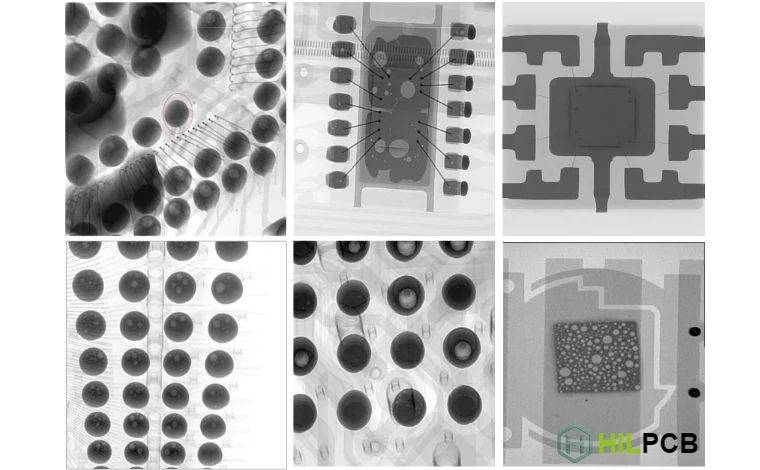
X-Ray Inspection: This is the final method to verify Low-void BGA reflow results. Because BGA joints are hidden under the package, X-Ray is the only non-destructive internal inspection technique. Advanced 2.5D or 3D AXI (automated X-ray inspection) systems can detect bridging, head-in-pillow (Head-in-Pillow), and other defects, while also calculating void ratio for each ball and comparing against IPC limits. These data are critical for optimizing the reflow profile (e.g., in vacuum reflow, setting vacuum timing and duration).
By integrating SPI and X-Ray data into Traceability/MES, manufacturers can build end-to-end traceability—from paste printing to final joint quality—providing strong assurance for high-end SMT assembly.
📊 Correlating BGA void ratio and reliability
Based on IPC-A-610 and IPC-7095, long-term electrical reliability is evaluated via the voided area percentage.
High-reliability class with strong thermal-fatigue life; suitable for aerospace, automotive, and medical core boards.
Reduced joint cross-section; potential overheating and cracking under high current or severe vibration.
Above IPC Class 2/3 limits—high risk of non-wet opens or early random failures.
Closed-loop inspection and data traceability across NPI EVT/DVT/PVT
New product introduction (NPI) is a structured journey from prototype to mass production, typically divided into engineering validation test (EVT), design validation test (DVT), and production validation test (PVT). SPI/AOI/X-Ray inspection plays different roles in each phase, together forming a data-driven quality closed loop.
EVT (engineering validation test): Focuses on feasibility and basic functionality. Volumes are low, but analysis is deep. X-Ray is often used for detailed evaluation of first articles—checking BGA joint formation, hybrid-stack-up registration, and more. AOI programs are also initially created and tuned. All inspection data are shared with design engineers as physical feedback for DFM/DFT/DFA review, guiding iterative design improvements.
DVT (design validation test): Validates all specifications and performance targets. Volumes increase and the process becomes more stable. SPI and AOI programs are refined to increase coverage and reduce false calls. X-Ray monitors stability of critical processes (e.g., BGA soldering). This stage emphasizes correlating inspection data with functional test (FCT) outcomes to identify the key manufacturing variables that affect performance.
PVT (production validation test): The final gate before mass production, validating line capability and process stability. At this point, SPI/AOI/X-Ray inspection is fully integrated into the production flow. Data are uploaded in real time to Traceability/MES for statistical process control (SPC), monitoring yield and defect trends. Success here marks readiness for high-volume, high-quality production. Through a data closed loop, NPI EVT/DVT/PVT ensures a smooth transition from design to manufacturing.
Advanced processes for complex through-holes and mixed assembly
Modern 5G/6G communication boards are not only carriers for RF and high-speed digital signals—they often include power modules, connectors, and other traditional through-hole components. This mixed SMT + THT requirement raises new demands for both process capability and inspection coverage.
Selective wave soldering: For high-density boards with only a small number of through-hole components, conventional full-board wave soldering re-heats already-mounted SMT parts (especially BGA), adding reliability risk. Selective wave soldering uses a movable mini solder nozzle to solder only targeted joints, avoiding unnecessary thermal exposure. However, the local process window is narrower and requires tight control. AOI and X-Ray inspection are critical to confirm proper fillets, detect bridging, and verify through-hole fill against IPC requirements.
Backdrill (Backdrill): To improve high-speed channel performance, backdrilling removes unused via stubs in multilayer boards. Stubs create reflections that can severely degrade signal integrity at mmWave frequencies. Depth control is key: too shallow leaves residual stub; too deep risks damaging functional layers. X-Ray inspection is one of the most effective ways to verify backdrill depth and quality non-destructively by confirming residual stub length is within spec.
These advanced processes further highlight why SPI/AOI/X-Ray inspection matters as a unified inspection platform. Whether SMT or THT, surface features or internal structures, this “inspection trio” provides comprehensive quality monitoring—supporting complex Turnkey PCBA delivery with robust assurance.
HILPCB core strengths in assembly and inspection
- ✅ End-to-end inspection coverage: from 3D SPI and inline AOI to 3D AXI—full-coverage monitoring across printing, placement, and soldering.
- ✅ Advanced process capability: deep expertise in Low-void BGA reflow, Selective wave soldering, and precision backdrilling—supporting complex mixed-assembly needs.
- ✅ Data-driven decision making: a powerful Traceability/MES system unifies all inspection data to support NPI EVT/DVT/PVT and continuous improvement in mass production.
- ✅ Expert-level DFM support: experienced engineers provide professional DFM/DFT/DFA review to mitigate risks early and optimize cost.
Conclusion
On the road from 5G to 6G, PCBs are no longer just carriers for components—they are the foundation of system performance. Managing low-loss and high-integration challenges in the mmWave era requires full collaboration across design, materials, fabrication, and assembly. SPI/AOI/X-Ray inspection is the “eyes” and “brain” of that collaboration: it provides far more than a pass/fail label—it delivers lifecycle data and actionable insight.
From early DFM/DFT/DFA review to mitigate design risks, to process validation and iteration across NPI EVT/DVT/PVT, to precision monitoring of critical processes such as Low-void BGA reflow and Selective wave soldering, this inspection trio is irreplaceable. By deeply integrating with Traceability/MES, HILPCB maximizes the value of SPI/AOI/X-Ray inspection, ensuring every 5G/6G communication PCB delivered achieves excellent performance and rock-solid reliability.
Common Questions
Why can’t a 5G or 6G communication board rely on AOI alone for quality judgment?
Because AOI mainly evaluates visible surface conditions. Many of the defects that threaten mmWave performance and long-term reliability are hidden inside BGA joints, under packages, or within complex through-hole structures, so SPI and X-ray are still necessary.
Why is low-void BGA reflow especially important in this class of product?
Voids reduce not only mechanical robustness but also the effectiveness of the thermal path. On dense, high-power communication devices, poor heat flow under the package raises temperature stress and increases the risk of early degradation.
Why do backdrilling and selective wave soldering also depend on a strong inspection loop?
Because both are narrow-window processes with expensive rework consequences. A small backdrill error can leave a harmful stub or damage a target layer, while selective wave soldering can miss fill or overheat nearby regions unless process data and inspection stay aligned.
Why should NPI teams connect inspection data into traceability and MES systems?
Because EVT, DVT, and PVT are valuable only if the team can quickly determine whether a problem came from design, materials, or process. Linking SPI, AOI, X-ray, and downstream electrical results shortens that learning loop dramatically.