
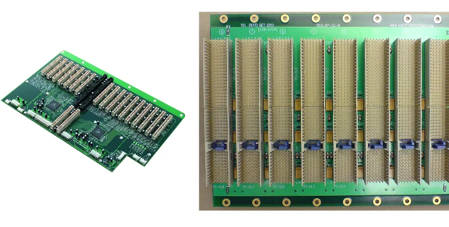
In the era of exponential growth in Artificial Intelligence (AI) and Machine Learning (ML), data center infrastructure is facing unprecedented performance pressure. As the core hub connecting computing, storage, and networking resources, the design and manufacturing complexity of the AI server backplane PCB has reached new heights. To carry ultra-high-speed signals of PCIe 5.0/6.0 or even higher generations, and to provide stable current for GPU/TPU accelerators with power consumption reaching thousands of watts, any minute manufacturing defect can lead to catastrophic system failure. Therefore, a rigorous, multi-level SPI/AOI/X-Ray inspection process is no longer optional, but the foundation of ensuring the stable operation of AI servers.
As an engineer focused on high-power density solutions, I know that every detail, from 48V VRM layout to high-speed connector Via design, directly affects the performance and reliability of the final product. Traditional quality control methods can no longer meet the demanding requirements of today's AI hardware. Only by systematically integrating 3D Solder Paste Inspection (SPI), Automated Optical Inspection (AOI), and X-Ray Inspection (AXI) can we capture and correct potential defects at every critical node of manufacturing, thereby delivering a standard-compliant industrial-grade AI server motherboard PCB. This article will examine the core technologies of SPI/AOI/X-Ray inspection, revealing how they safeguard the integrity of the complex AI server motherboard PCB stackup, and ultimately achieve superior AI server motherboard PCB quality.
Why is Multi-Level Inspection Critical for AI Server PCB?
The AI server backplane is the "backbone" of the entire system; it not only has to process differential signals up to 64 GT/s but also carry hundreds of amperes of DC current. This dual extreme environment of electrical and physical conditions places nearly harsh requirements on PCB manufacturing precision. A tiny solder joint void, an offset BGA solder ball, or an incompletely filled Plated Through Hole (PTH) can all become sources of signal reflection, power noise, or thermal failure.
Traditional single-point inspection, such as relying solely on AOI, cannot see through the solder joint conditions under bottom-terminated packages like BGA or QFN, nor can it assess the structural integrity inside the multilayer board. This is why a closed-loop quality control system integrating SPI/AOI/X-Ray inspection is so important. It follows the principle that "defect prevention is better than defect detection":
- Source Prevention (SPI): Before component placement and reflow soldering, by precisely measuring the volume, area, and height of the solder paste, welding defects caused by poor solder paste printing are eliminated at the source. This step accounts for over 60% of the causes of all soldering defects.
- Process Monitoring (AOI): After reflow soldering, quickly check the placement position, polarity, absence, or error of components to ensure all surface components meet design specifications.
- Deep Verification (X-Ray): Penetrates components and the PCB to perform non-destructive testing on solder joints under packages like BGA and LGA, checking for hidden defects such as voids, bridging, and Head-in-Pillow effects, and verifying the filling quality of vias.
This layered, progressive inspection strategy ensures that the entire process from solder paste printing to final soldering formation is under control, which is the only way to achieve high-reliability AI server motherboard PCB quality.
The First Line of Defense: The Core Role of 3D Solder Paste Inspection (SPI)
In the SMT (Surface Mount Technology) process, solder paste printing is the first and most critical link determining the final soldering quality. 3D SPI (Solder Paste Inspection) uses laser triangulation principles to perform precise three-dimensional morphological measurements on every solder paste deposit printed on the PCB pads. It is not just checking for presence or absence, but quantitative analysis.
The SPI system detects the following key parameters:
- Volume: Is the amount of solder paste too much or too little? Too much may lead to bridging shorts after soldering, while too little may cause cold solder joints or open circuits.
- Area: Is the area of solder paste covering the pad sufficient? Insufficient coverage affects soldering strength.
- Height: Are the average and maximum heights of the solder paste within the process window? Uneven height may cause components to tilt or shift during the reflow process.
- Offset: Is the center of the solder paste aligned with the center of the pad? Severe offset leads to component skewing.
- Shape: Is the shape of the solder paste regular? Abnormal shapes (such as slumping, peaking) indicate problems with the printing process.
For the dense 0.4mm pitch BGA and high-density connectors on the AI server backplane, precise solder paste control is critical. By monitoring these parameters in real-time, the SPI system can issue alerts before defects solidify (reflow soldering), allowing production engineers to immediately adjust printer parameters (such as squeegee pressure, speed, separation parameters), thereby achieving closed-loop process control. This not only significantly reduces the rework rate but also guarantees the soldering consistency required for an industrial-grade AI server motherboard PCB from the source.
How Automated Optical Inspection (AOI) Ensures Component-Level Precision?
When the PCB passes through the reflow oven, all surface mount components have been soldered in place. At this point, Automated Optical Inspection (AOI) equipment takes over the next leg of quality control. AOI uses high-resolution cameras, multi-angle light sources (including colored and monochromatic light), and complex image processing algorithms to compare captured images with pre-programmed acceptance standards based on Gerber and BOM data.
AOI excels at detecting the following surface defects:
- Missing or Extra Components: Checks if components are unmounted or if there are extras.
- Position Offset and Rotation: Whether the component is precisely located at the center of the pad.
- Polarity Errors: For directional components like diodes, electrolytic capacitors, and ICs, whether their orientation is correct.
- Wrong Part: Based on the silkscreen or color code on the component surface, judges whether the wrong part was used.
- Soldering Quality: Checks if solder joints are full, and if there are issues like bridging, solder balls, or cold solder joints (preliminarily judged by solder joint color and shape).
- Optical Character Recognition (OCR): Reads the silkscreen on components to double-check against the BOM.
In the assembly process of the AI server backplane, the VRM (Voltage Regulator Module) area is filled with a large number of MOSFETs, inductors, and capacitors; an error in any single component can lead to power rail failure. Meanwhile, the placement precision of tiny components like coupling capacitors and termination resistors on high-speed signal links directly affects signal integrity. AOI can complete these checks with speed and precision far exceeding the human eye, making it a key technology for ensuring consistency in large-scale, high-density assembly. However, AOI's line of sight is limited to the surface; for defects hidden under packages, more powerful tools are needed.
Comparison of SPI, AOI, and X-Ray Capabilities
| Inspection Technology | Inspection Stage | Main Inspection Objects | Core Advantages | Limitations |
|---|---|---|---|---|
| 3D SPI | Pre-Reflow | Solder paste volume, area, height, offset | Prevents soldering defects at the source, provides process control data | Cannot detect post-soldering defects |
| AOI | Post-Reflow | Component missing/offset/polarity, surface solder joints, silkscreen | Fast speed, suitable for mass production, high efficiency in detecting surface defects | Cannot detect bottom solder joints like BGA/LGA |
| X-Ray (AXI) | Post-Reflow / Final Inspection | BGA/CSP solder joint voids, bridging, opens, PTH fill, internal traces | The only non-destructive method to detect hidden solder joints, provides deep analysis | Slower speed, higher cost, usually used for sampling or 100% inspection of critical devices |
Revealing Hidden Defects: The Ultimate Power of X-Ray Inspection (AXI)
X-ray inspection (Automated X-ray Inspection, AXI) is the "ultimate weapon" in the SPI/AOI/X-Ray inspection system. Since X-rays can penetrate silicon chips, plastic packages, and PCB substrates, they can clearly reveal the morphology of solder joints hidden underneath components. For the PCIe switch chips, FPGAs, and high-current connectors packaged in BGA widely used on AI server backplanes, AXI is the only effective non-destructive testing method.
AXI technology is mainly divided into several types:
- 2D X-Ray: Provides a flat, top-down perspective image, which can quickly discover obvious defects such as bridging and missing solder balls.
- 2.5D X-Ray (Angled View): By tilting the detector or the sample to observe from different angles, it can better distinguish overlapping solder joints and help judge defects like Head-in-Pillow.
- 3D X-Ray (CT Scan): Generates a complete three-dimensional model by rotating the sample 360 degrees and performing tomographic reconstruction. This is the most powerful AXI technology, capable of precisely measuring the voiding rate of BGA solder joints, analyzing the copper fill quality of PTH vias, and even checking for delamination or cracks inside the PCB.
In AI server applications, the voiding rate of BGA solder joints is a key indicator. Excessive voiding reduces the thermal conductivity and mechanical strength of the solder joint, forming hot spots under high-power GPU chips, which may lead to thermal fatigue failure over long-term operation. At the same time, voids also affect the impedance continuity of high-speed signals. The IPC-A-610 standard has clear acceptance criteria for solder joint voids (e.g., Class 3 requires the void area not to exceed 25% of the total area), and only 3D AXI can provide precise quantitative data to ensure the product meets AI server motherboard PCB compliance requirements. Professional manufacturers like Highleap PCB Factory (HILPCB) use advanced 3D AXI equipment to perform 100% inspection on all critical BGAs, ensuring absolute safety.
Integrating SPI/AOI/X-Ray for a Zero-Defect Manufacturing LoopSingle inspection technologies can only solve partial problems, but integrating SPI/AOI/X-Ray inspection into a unified quality management platform maximizes effectiveness. An advanced Manufacturing Execution System (MES) can correlate data from these three, forming a powerful process control closed loop.
The workflow of this closed loop is as follows:
- SPI detects anomaly: SPI detects low solder paste volume on multiple consecutive pads.
- System automatic warning: The MES system immediately issues an alert to the printer and may automatically pause the production line.
- Root cause analysis: Engineers analyze the data and discover it is caused by clogged stencil apertures.
- Correction and prevention: After cleaning the stencil, SPI data returns to normal. Meanwhile, the system records this event to optimize the automatic stencil cleaning cycle.
- Data traceability: AOI or AXI detects a cold solder joint defect on a BGA in a subsequent process. Through the MES system, the solder paste data of that PCB at the SPI station can be traced to analyze the correlation between the two, thereby optimizing SPI inspection thresholds.
In this way, defects are not just "picked out," but "prevented." This data-driven smart manufacturing mode is core to improving the first pass yield and long-term reliability of complex PCB products (such as HDI PCB). It transforms AI server motherboard PCB quality from a vague concept into a series of measurable, controllable, and traceable precise indicators.
🔍 HILPCB Integrated Inspection Implementation Process
Through a multi-dimensional closed-loop inspection system, achieving full-process quality monitoring from digital modeling to finished product rollout.
Digitally parsing design files, automatically synchronizing generation of inspection reference programs.
Real-time monitoring of solder paste printing height, volume, and area, intercepting printing defects.
High-precision visual recognition of component misalignment, omission, and polarity reversal, verifying surface soldering quality.
Penetrative imaging, deeply verifying internal BGA and Through-Hole (PTH) soldering status.
Aggregating big data from inspection, driving continuous iterative optimization of front-end manufacturing processes.
How Does Inspection Data Verify AI Server Motherboard PCB Stackup Design?
A carefully designed AI server motherboard PCB stackup is the foundation for ensuring Signal Integrity (SI) and Power Integrity (PI). However, the design ultimately needs to be perfectly realized through manufacturing. Data provided by SPI/AOI/X-Ray inspection can conversely verify the manufacturability of the Stackup design and its degree of realization in actual production.
For example, a complex AI server motherboard PCB stackup may contain more than 20 layers, use multiple sequential lamination cycles, and extensively employ Back-Drilling and blind/buried Via technologies. X-ray inspection plays a key role in this:
- Verifying Back-Drilling depth: X-ray can measure the length of Via Stub, ensuring the Back-Drilling process accurately removes excess copper barrels, thereby minimizing reflection of high-speed signals.
- Checking blind/buried Via alignment: For HDI structures, X-ray can check the alignment accuracy between layers and the connection between laser drills and inner layer pads.
- Evaluating plating fill quality: For power Vias that need to carry high currents, 3D X-Ray can quantify the plated copper fill rate inside the Via, ensuring there are no voids or cracks, guaranteeing a low-impedance current path.
These real data from the manufacturing floor provide valuable feedback for design engineers. If inspection reveals that the fill rate of Vias with a specific structure is generally low, engineers can adjust Via sizes or pad designs in the next design revision to improve manufacturability. This close collaboration between design and manufacturing is key to creating high-performance high-speed PCB.
Achieving AI Server Motherboard PCB Compliance Through Verifiable Data
In enterprise and data center applications, product compliance is critical. AI server motherboard PCB compliance is not just about meeting electrical performance metrics, but also includes adherence to industry standards such as IPC-A-610 (Acceptability of Electronic Assemblies), especially the most stringent Class 3 level.
Class 3 standards apply to high-reliability applications such as life support, aerospace, and high-performance servers. It has extremely strict regulations on soldering, component placement, cleanliness, etc. Traditional visual inspection is highly subjective and difficult to provide consistent and traceable evidence. Whereas SPI/AOI/X-Ray inspection systems provide objective, quantifiable data reports.
Every inspected PCB can generate a detailed report recording SPI measurement values, AOI images, and AXI analysis results (such as voiding rates) for all critical solder joints. These reports become part of the product quality archive, which can be used not only for internal process control but also as strong evidence that the manufacturing process complies with specifications during customer audits or field failures. The turnkey assembly service provided by HILPCB includes complete traceability reports, ensuring that every shipped circuit board meets strict AI server motherboard PCB compliance requirements.
HILPCB Manufacturing Capabilities: Born for AI Server Backplanes
| Technical Parameters | HILPCB Capabilities | Value for AI Servers |
|---|---|---|
| Max Layer Count | 64+ Layers | Supports ultra-complex high-speed signal and power layering design |
| Board Thickness | Up to 12mm | Meets the needs of high-current, high-rigidity [backplane PCB](/products/backplane-pcb) |
| Impedance Control Accuracy | ±5% | Ensures signal integrity for high-speed differential pairs like PCIe 5.0/6.0 |
| Back-Drilling Depth Control | ±0.05mm | Minimizes Via Stub, reducing signal reflection |
| High-Frequency Materials | Megtron 6/7, Tachyon 100G, Rogers, etc. | Provides ultra-low loss dielectrics, supporting 224Gbps+ signal transmission |
Beyond Inspection: The Ultimate Protection of Conformal Coating
Even if a PCB passes all SPI/AOI/X-Ray inspection perfectly, its lifecycle has just begun. In the harsh operating environment of data centers, dust, moisture, chemical contaminants, and temperature fluctuations can pose long-term threats to the circuit board. To ensure the reliability of 24/7 uninterrupted operation, Conformal coating becomes a critical protective barrier.Conformal coating is a thin, transparent polymeric coating that is uniformly applied to the surface of the assembled PCB, forming a tough protective film. This film can:
- Moisture and humidity protection: Prevents moisture intrusion that leads to corrosion of metal traces or a decrease in insulation resistance.
- Dust and contaminant protection: Prevents conductive dust particles from causing short circuits between pins.
- Enhanced mechanical strength: Provides additional mechanical support for solder joints and component pins, enhancing resistance to vibration and shock.
- Improved insulation performance: Increases the creepage distance between conductors, preventing arc discharge under high voltage.
For industrial-grade AI server motherboard PCBs deployed in various environments, selecting the appropriate Conformal coating material (such as acrylic, silicone, polyurethane) and employing precise application processes (such as selective spraying, dipping) is a critical step in extending product life and reducing field failure rates. It is the final external protection provided for the product after all rigorous internal inspections.
Conclusion: Choosing a Manufacturing Partner with Comprehensive Inspection Capabilities
The manufacturing of AI server backplanes is a systematic engineering feat integrating material science, high-speed circuit design, precision manufacturing, and strict quality control. In this complex chain, a comprehensive SPI/AOI/X-Ray inspection strategy acts as the bridge connecting design with reliability and is the "gatekeeper" ensuring final product performance meets standards. It not only detects and eliminates defects but also continuously optimizes the entire manufacturing process through a data-driven approach, thereby systematically enhancing AI server motherboard PCB quality.
From SPI precisely controlling solder paste deposition, to AOI comprehensively inspecting surface components, to X-Ray deeply probing internal solder joints, every step is indispensable. Only when these technologies are combined with advanced AI server motherboard PCB stackup design and reliable Conformal coating protection processes can top-tier products meeting strict AI server motherboard PCB compliance standards be ultimately created.
Choosing a partner like Highleap PCB Factory (HILPCB), which not only possesses advanced manufacturing equipment but also deeply integrates SPI/AOI/X-Ray inspection into its production process, means you are choosing certainty, reliability, and a shared commitment to excellence.
If you are looking for a PCB manufacturing and assembly partner capable of mastering complexity and ensuring zero defects for your next-generation AI servers, please contact us immediately. Let us safeguard your innovation with industry-leading inspection technologies and manufacturing capabilities.