
In high-availability systems such as data centers, telecom base stations, and industrial automation, power and cooling systems are the lifeline ensuring business continuity. As power density continues to climb, the PCBs in these systems face unprecedented electrical and thermal stress challenges. To address these challenges, every link from design to manufacturing must pursue ultimate reliability. Among them, the manufacturing process quality control system centered on SPI/AOI/X-Ray inspection is key to ensuring the perfect realization of advanced functions like redundancy, hot-swap, and intelligent monitoring. It is not only a tool for discovering defects but also the foundation for verifying design, optimizing processes, and guaranteeing product reliability throughout its lifecycle. A comprehensive quality strategy, combining early DFM/DFT/DFA review with strict inspection during production, and finally verified through First Article Inspection (FAI), ensures that every delivered PCBA meets the most stringent standards.
DFM/DFT/DFA Review: Laying the Foundation for High-Reliability Manufacturing at the Source
Before discussing any specific inspection technologies, the importance of the design phase must be emphasized. An excellent power system design, if it cannot be manufactured efficiently and reliably, will have its value greatly discounted. This is exactly where the core value of DFM/DFT/DFA review (Design for Manufacturing/Test/Assembly review) lies. For high-power PCBs, this review process is particularly critical, as it directly affects the efficiency and effectiveness of subsequent SPI/AOI/X-Ray inspection.
DFM/DFT/DFA review focuses on the following key aspects:
- Electrical Safety and Spacing: Reviewing creepage and clearance between high-voltage and low-voltage circuits to ensure compliance with safety standards like UL and IEC, preventing arcing and short circuits. This provides a clear judgment baseline for subsequent AOI inspection.
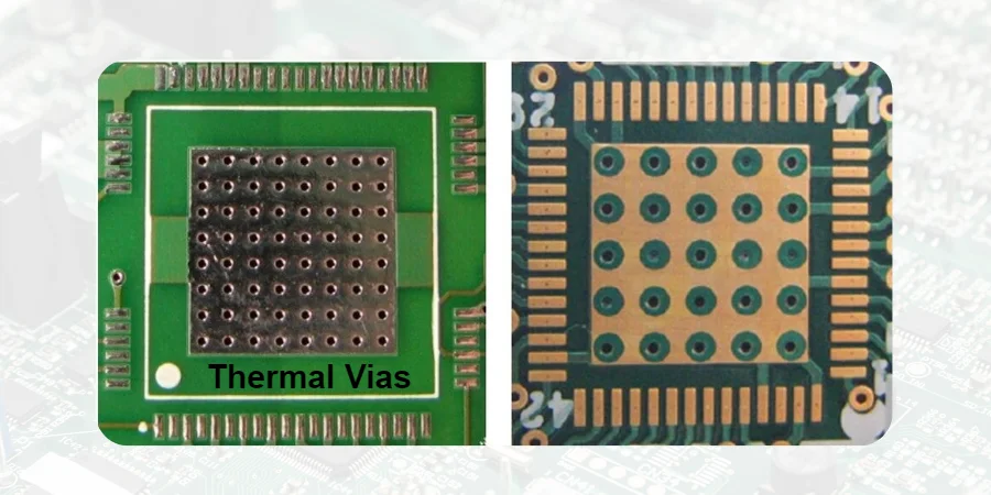
- Thermal Management Design: Evaluating whether the layout of thermal vias, large copper areas, and Heavy Copper PCB is reasonable, to ensure heat from power devices (such as MOSFETs, IGBTs) can be effectively conducted away. Reasonable design enables X-Ray to more accurately assess the voiding rate of critical solder joints.
- Testability (DFT): Planning test points for critical nodes to ensure voltage, current, and PMBus signals can be automatically tested during production. Without good DFT design, functional verification may become a bottleneck even if all optical and X-Ray inspections are passed.
- Assemblability (DFA): Evaluating the pad design and layout of heavy components (such as large inductors, busbars, connectors) to ensure their mechanical stability and soldering reliability. This is directly related to the quality of the THT/through-hole soldering process.
By conducting a thorough DFM/DFT/DFA review early in the design stage, we not only prevent potential manufacturing defects but also ensure that the PCB design itself is "inspectable". This lays a solid foundation for the smooth implementation of subsequent automated inspection processes and solidifies design rules into the production flow through the Traceability/MES system.
Implementation Process: Interaction of DFM Review and Manufacturing Inspection
- Design Input and Rule Definition: Customers provide Gerber, BOM, and schematics. HILPCB engineers define DFM/DFT/DFA inspection rules based on power, voltage, and safety requirements.
- Automated Analysis and Manual Review: Use professional software for automated analysis, and experienced engineers manually review critical power paths, thermal designs, and high-density areas.
- Issue Reporting and Collaborative Modification: Generate detailed DFM reports, communicate potential manufacturing risks with customers, and propose optimization suggestions.
- Rule Import into MES System: Finalized design rules are imported into the Traceability/MES system to guide production and serve as the judgment basis for SPI/AOI/X-Ray inspection.
- Closed-loop Feedback: Inspection data from production is fed back to the design department to continuously optimize future DFM rule libraries.
SPI/AOI/X-Ray Inspection: Ensuring Manufacturing Precision for Hot-Swap and Surge Suppression Circuits
Hot-swap functionality allows modules to be replaced without powering down the system and is the core of high-availability systems. Its circuits typically contain MOSFETs, controller ICs, TVS diodes, and precision shunt resistors for suppressing inrush current. Any manufacturing defect in these components can lead to system crashes or permanent damage when a module is inserted. The trinity inspection strategy of SPI/AOI/X-Ray inspection provides the ultimate guarantee for the reliability of these critical circuits.
- SPI (Solder Paste Inspection): Everything starts with solder paste. For power MOSFETs in hot-swap circuits, their thermal pads require precise and sufficient solder paste volume. SPI uses 3D scanning to precisely measure the volume, area, and height of solder paste on each pad. Excessive solder paste may lead to short circuits or component shifting after soldering; too little will cause cold solder joints or poor heat dissipation, causing the MOSFET to fail due to overheating when suppressing inrush current.
- AOI (Automated Optical Inspection): After reflow soldering, AOI takes over the task of detecting surface defects. It can quickly identify:
- Component Shifting and Rotation: Ensuring MOSFETs, controllers, and passive components are precisely located on the pads.
- Polarity Errors: The directionality of TVS diodes, electrolytic capacitors, and ICs is critical. A reversed TVS diode will fail to provide surge protection.
- Soldering Defects: Surface-visible issues such as insufficient solder, solder bridging, and tombstoning.
- Foreign Objects and Contamination: Checking board cleanliness to prevent conductive foreign objects from causing short circuits.
- X-Ray (X-Ray Inspection): For QFN package controller ICs and power MOSFETs with bottom pads, as well as complex power management chips in BGA packages, AOI is powerless. X-Ray inspection is the only means to "see through" these components and check their internal soldering quality. It can clearly reveal:
- Solder Joint Voiding: This is one of the most fatal defects in power device solder joints. Voids significantly increase the thermal resistance and electrical resistance of the solder joint, leading to local overheating, accelerating device aging, and ultimately failing under peak loads. Industry standards (such as IPC-A-610) have strict regulations on voiding rates.
- Internal Short Circuits: Detecting potential shorts between BGA solder balls or QFN pads.
- Solder Wetting: Assessing the bonding between solder and pads.
Before launching large-scale SMT Assembly, a strict First Article Inspection (FAI) process ensures that every detail of the first article has passed all the above inspections, thereby verifying that the entire production line setup is correct.
OR-ing and Redundant Power Supply: How Inspection Technology Ensures Reliability of Ideal Diodes and Current Sharing Circuits
N+1 or N+N redundancy is the standard configuration for power systems, centered on the OR-ing circuit, which is used to combine the outputs of multiple power modules onto a shared power bus while isolating faulty modules. Traditional diode OR-ing solutions are gradually being replaced by MOSFET-based "ideal diode" solutions due to high voltage drop and high power consumption. These solutions impose higher requirements on manufacturing quality.
Ideal diode controllers combined with high-current MOSFETs can achieve extremely low conduction voltage drops, but their control circuits are relatively complex, and the soldering quality of power MOSFETs directly determines the success or failure of the entire redundancy scheme.
- Role of AOI: Ensuring that the ideal diode controller IC and external MOSFETs are installed in the correct orientation. A misoriented MOSFET may cause reverse current flow or fail to disconnect effectively during a fault, rendering the redundant design useless.
- Critical Role of X-Ray: Power MOSFETs typically use packages with large thermal pads. X-Ray inspection is critical for evaluating the soldering quality of these pads. Excessive voids inside the solder joint will significantly increase the on-resistance (Rds(on)), not only reducing efficiency but also generating serious hotspots under high current, eventually causing the MOSFET to burn out and endangering the entire power bus.
- Challenges of THT/through-hole soldering: For busbars and high-current connectors that need to carry hundreds of amperes of current, the THT/through-hole soldering process is usually adopted. Inspecting the barrel fill of these through-hole solder joints is equally important. X-Ray can be used to check the solder filling of through-holes, ensuring low impedance and high mechanical strength of the connection, which is vital for the thermal and electrical performance of High-Thermal PCB.
Key Takeaways: Core Focus Points in Redundant Power Supply Manufacturing
- Ideal Diode MOSFET Soldering: The void rate of thermal pads must be strictly controlled via X-Ray, with a target typically below 25%.
- Current Sharing Circuit Precision: Precision resistors used for current sharing must have consistent solder joint quality; SPI inspection ensures high consistency of solder paste volume.
- High-Current Connector Soldering: Whether SMT or THT, the soldering quality of connectors requires focused attention to prevent overheating caused by excessive contact resistance.
- Controller IC Integrity: Controllers in BGA or QFN packages must be checked via X-Ray to ensure there are no internal shorts or opens.
PMBus Monitoring and System Telemetry: Potential Impact of Manufacturing Defects on Data Integrity
Modern power supply systems have long surpassed simple energy conversion. Through protocols like PMBus (Power Management Bus), they achieve real-time monitoring, alarming, and remote adjustment of key parameters such as voltage, current, power, and temperature. This intelligent management greatly enhances system maintainability (MTTR) and overall reliability. However, all of this relies on precise telemetry data, and manufacturing defects are potential killers of data integrity.
- Interference on Communication Lines: PMBus signal lines are typically low-speed digital signals, but if manufacturing defects such as tiny solder beads or flux residues exist near their routing paths, leakage paths may form under specific temperature and humidity conditions. This can interfere with communication, leading to data errors or bus hang-ups. AOI and X-Ray inspection can detect these potential short-circuit risks.
- Accuracy of Sensing Components:
- Current Sense Resistors: Shunt resistors used for current measurement are typically low-resistance precision components. Any flaw in their solder joints (such as cold solder joints or voids) will introduce extra parasitic resistance, leading to inaccurate current readings, which in turn affects power calculations and overcurrent protection thresholds. SPI and X-Ray inspection are critical for ensuring their soldering consistency.
- Temperature Sensors: NTC thermistors or temperature sensing diodes used to monitor hotspot areas cannot accurately reflect the true temperature of the device if poorly soldered. This may lead to failure of cooling fan strategies or delayed over-temperature protection.
- Value of Traceability/MES: When field equipment reports abnormal PMBus data, a powerful Traceability/MES system plays a huge role. By entering the device's serial number, we can trace its entire production history, including original images and data from SPI/AOI/X-Ray inspection. For example, we can view the SPI solder paste volume data for a specific current sense resistor or the X-Ray void rate image of its power MOSFET, thereby quickly pinpointing whether the root cause is a design defect, component failure, or manufacturing process deviation.
After all inspections and tests are completed, applying a layer of Conformal coating can effectively protect these sensitive monitoring circuits from moisture, dust, and chemical erosion, further ensuring their long-term operational reliability.
Reliability Verification and Life Assessment: The Quality Closed Loop from MTBF to Accelerated Testing
MTBF (Mean Time Between Failures) is a key metric for measuring system reliability, but it is a theoretical prediction based on design and component data. Turning theory into reality relies on a controllable and repeatable manufacturing process. The data provided by SPI/AOI/X-Ray inspection is the bridge connecting theoretical reliability with actual product life.
- Quantifying Process Capability: By continuously monitoring solder paste volume distribution (Cpk) measured by SPI, defect rates (DPMO) detected by AOI, and void rates measured by X-Ray, we can quantify the stability and capability of the production process. A stable and capable process is the prerequisite for producing high-reliability products.
- Basis for Accelerated Life Testing (ALT): When conducting accelerated life tests such as thermal cycling, vibration, or damp heat, manufacturing defects are the primary cause of early failures. For example, a PCBA with a high solder joint void rate will experience solder joint fatigue and cracking faster during thermal cycling tests due to mismatches in the coefficient of thermal expansion (CTE) of materials. Screening for samples with low void rates via X-Ray for testing allows for a more accurate assessment of the design's intrinsic life.
- Importance of First Article Inspection (FAI): First Article Inspection (FAI) is the starting point of the entire quality verification. It is not just checking if the first product meets specifications, but a comprehensive verification of the entire manufacturing process (including THT/through-hole soldering and SMT). Passing FAI means we have confidence to proceed with mass production using the same process parameters.
- Final Protection: After all functional tests and reliability verifications are completed, Conformal coating, as the final process step, provides the PCBA with a sturdy barrier against external environmental erosion, significantly extending its service life in harsh environments.
HILPCB Manufacturing Capabilities Overview
Inspection Capabilities Technical Specifications Value for Power Systems 3D SPI Solder paste volume/area/height inspection, accuracy < 2µm Ensures thermal and electrical performance of power device solder joints 3D AOI Multi-angle cameras, capable of detecting 01005 components, coplanarity inspection Prevents component polarity errors and shifts, safeguarding control circuit functionality 3D X-Ray (AXI) CT tomography, calculates BGA/QFN void rates, checks through-hole fill Eliminates hidden soldering defects, ensuring long-term reliability Traceability/MES Component-level traceability, linked with inspection equipment data Achieves full-process quality monitoring and rapid failure analysis
Conclusion
In power supply and cooling systems requiring high power density and high reliability, PCB design and manufacturing quality are inseparable. An advanced redundant or hot-swap scheme will lose all its design advantages if its implementation carrier—the PCBA—has manufacturing defects. Therefore, a comprehensive quality control strategy centered on SPI/AOI/X-Ray inspection and integrated throughout the entire Turnkey PCBA Assembly process is indispensable.
From the DFM/DFT/DFA review in the design phase to the First Article Inspection (FAI) before production, through the three key inspections during the production process, and the full traceability achieved via the Traceability/MES system, finally supplemented by the ultimate protection of Conformal coating, this series of measures collectively forms a solid barrier for high-reliability PCBA manufacturing. At HILPCB, we deeply understand that the quality of every solder joint relates to the stable operation of your system. We use industry-leading inspection equipment and a strict quality management system to ensure that every PCBA delivered to you can work stably and reliably in the harshest environments, safeguarding your business.